Market Minds Advisory
Wafer Inspection Market

Wafer Inspection Market: Wafer Inspection Market. AI-Enabled Defect Classification Reshapes a Capex-Driven Fab Equipment Cycle

Fabs racing to qualify sub-3-nanometer nodes are pushing inspection equipment vendors past optical-only detection architectures, straining tool sets never engineered to resolve defects at today's shrinking critical dimensions across major foundry programs.

Lead Analyst

Published

September 2026

Make Smarter Decisions with Customized Research Insights

Request a free sample report and evaluate market opportunities, growth trends, and competitive dynamics relevant to your business needs.

2025 MARKET VALUE$7.5BMarket Size 2025
2036 FORECAST VALUE$20.4BBase Case , 2026 to 2036
CAGR 2026 TO 20369.5 %Bull 10.8% / Bear 8.2%
INCREMENTAL OPPORTUNITY$12.1BNet 10- year value creation
EXPANSION MULTIPLE2.48x2036 value over 2026 base
Strategic Levers
M&A Pipeline
Regional Outlook
Country Rankings
Competitive Intelligence
Segmental Deep-dive
Call-Us : 91 93563 13602

Executive Snapshot and Market Trajectory.

Wafer inspection demand is shifting from optical-only detection architectures toward AI-enabled automated classification systems, as fabs push vendors past the resolution limits most tools were originally engineered around. This transition is forcing equipment makers to rethink algorithm-centric roadmaps across nearly every major leading-edge fab nationwide.
AI-enabled automated defect classification systems lead segment growth as fabs pursue faster yield ramp decisions, even as legacy trailing-edge fabs continue relying on conventional bright-field optical tools for routine mature-node monitoring. East Asia absorbs the largest share of global demand, reflecting the region's dense concentration of leading-edge foundry capacity and memory fab construction. Fabs nationwide continue standardizing inspection architecture around automated classification as advanced node adoption accelerates rapidly.
Competition concentrates among a handful of diversified equipment majors controlling installed tool base and fab relationship depth, alongside specialty inspection developers that compete on defect sensitivity and throughput sophistication. Rising advanced node adoption and AI chip demand are reshaping vendor economics well beyond legacy optical-only offerings, while precision optics component cost volatility and qualification engineering talent availability continue to complicate margin planning across smaller regional suppliers. This pattern persists across most major regional fab programmes.
Market Definition
The wafer inspection market covers equipment and systems used to detect, classify, and review defects on semiconductor wafers during fabrication, including bright-field optical wafer inspection systems, dark-field optical wafer inspection systems, e-beam wafer inspection systems, patterned wafer defect review systems, unpatterned wafer inspection systems, and AI-enabled automated defect classification systems. The market excludes general lithography exposure and patterning equipment, standalone wafer probing and electrical test equipment without defect imaging capability, and general fab automation software without integrated inspection or metrology functionality.
Base Year Value
$7.5B in 2025 (MMA Primary Research Dataset, September 2026)
Forecast Period
2026 to 2036, eleven discrete annual values
CAGR
9.5% base case. Bull 10.8%. Bear 8.2%.
Fastest Growth Segment
AI-Enabled Automated Defect Classification Systems: 16.0% CAGR
Fastest Growth Country
China: 11.0% CAGR
Fastest Growth Region
South Asia and Pacific: 11.5% CAGR
Largest Region
East Asia: 38% of 2025 global value
Market Leaders
KLA Corporation, Applied Materials, Hitachi High-Tech, Onto Innovation, and Nova Ltd lead the field. Source: MMA Analysis based on company disclosures.
Primary Survey
n=3,800 procurement and R&D decision-makers, Q4 2025, six countries
Methodology
Demand-side build-up, cross-validated against public data, 47 expert interviews

Wafer Inspection Market Forecast Scenarios

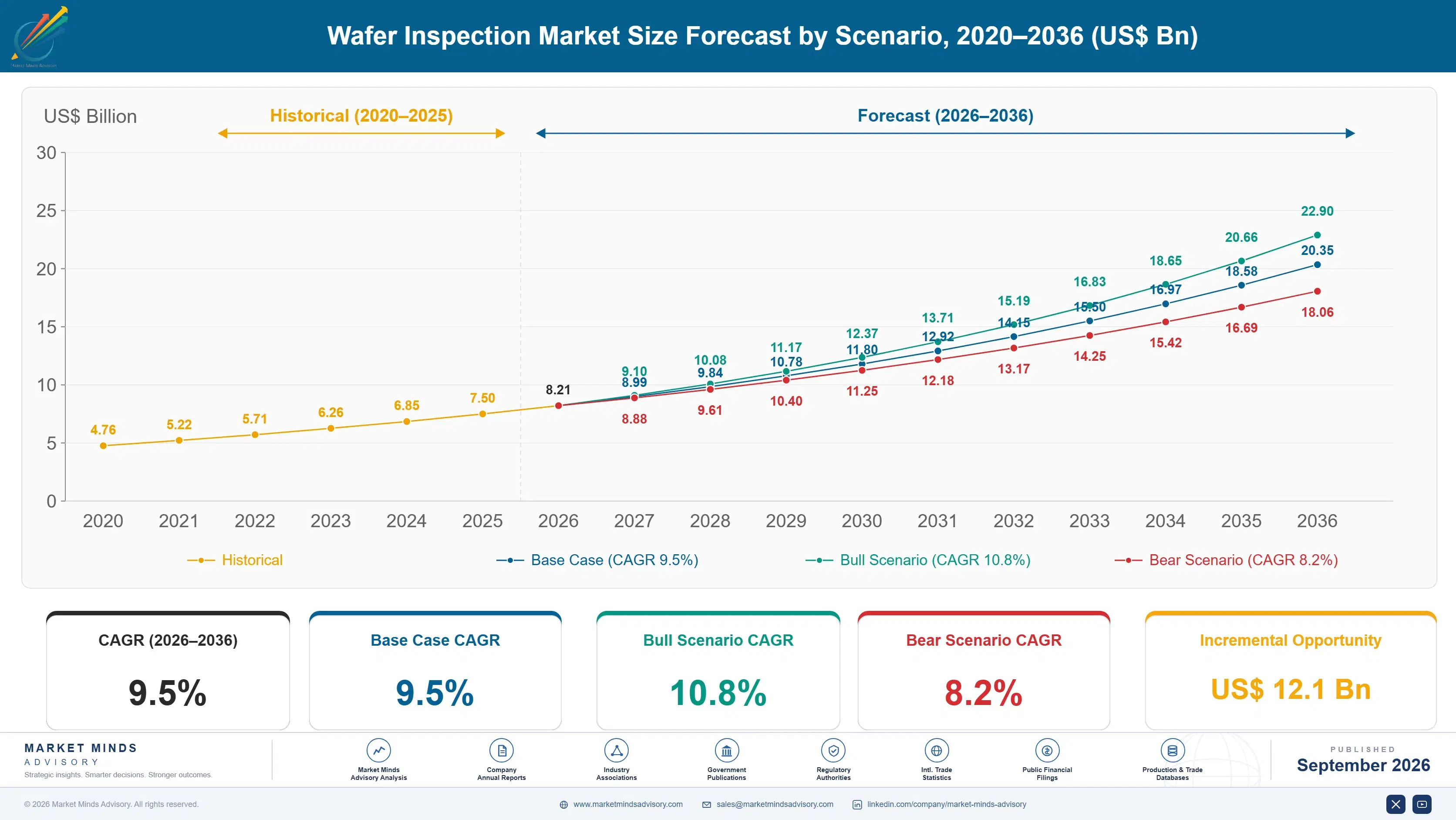
wafer-inspection-system-market-size-forecast-scenario-1789999438973
Between 2020 and 2025 wafer inspection demand grew at roughly 8.0 percent a year, steady as leading-edge foundry capex and established memory fab construction expanded gradually across mature optical inspection channels. Growth accelerated from 2023 as AI chip demand and sub-3-nanometer node qualification pulled category demand toward automated classification formats. That shift accelerated as additional vendors expanded dedicated algorithm development nationally.
The base case assumes continued growth as three mechanisms compound: fabs increasingly specifying automated classification systems to achieve faster yield ramp without expanding manual review headcount per fab; foundries expanding advanced node qualification programmes that require reliable, high-sensitivity inspection deployable across distributed production lines; and vendors introducing improved e-beam architecture that reduces false-detection rates without raising throughput cost. These mechanisms reinforce each other as advanced node adoption and AI chip demand continue compounding across major foundry and memory markets.
The bull case turns on faster-than-expected leading-edge fab capacity expansion across major East Asian and North American programmes. The bear case centers on sustained precision optics component cost volatility, which has historically delayed vendor tool qualification and slowed new platform investment across smaller regional suppliers facing thinner capital budgets. Diversified suppliers navigate this volatility more effectively than narrowly focused competitors.

Automated Classification Reshapes Equipment Vendor Economics

Wafer inspection sits at the intersection of precision optics engineering, semiconductor node transition trends, and shifting AI chip yield requirements. As automated classification formats spread, vendors increasingly compete on documented defect sensitivity and false-detection accuracy rather than tool price alone, even where standard optical tools carry a substantial cost advantage over automated alternatives across most established trailing-edge categories today. This dynamic is reshaping vendor strategy across major foundry and memory markets.
MARKET CONCENTRATIONCR5: 68%Ownership concentrates heavily among a handful of diversified equipment majors
AVERAGE TOOL SELLING PRICE$4.2 million per high-sensitivity inspection systemPricing varies sharply by resolution capability and throughput tier
AI CLASSIFICATION PENETRATION29 percent of installed inspection tool volumeAutomated classification formats represent a growing minority of installations overall
TOP PRODUCING COUNTRY SHARETaiwan: 33 percent of global fab tool installationsInstallation volume concentrates near established leading-edge fab clusters
AVERAGE TOOL UTILIZATION RATE87 percent across active production fab linesUtilization varies meaningfully by fab maturity and node generation
PRECISION OPTICS COST SHARE26 percent of cost of goods soldOptical component pricing directly affects overall vendor profitability margins
Commercially the category concentrates among a handful of diversified equipment majors offering integrated tool base and fab relationship capability, alongside specialty inspection developers that compete on sensitivity depth. Diversified majors compete on installed fab base breadth and multi-node platform scale, while specialty developers win on defect sensitivity and application-specific customization depth, since logic, memory, and advanced packaging applications each demand distinct resolution and throughput specifications.
The next decade will be shaped by continued automation premiumization, expanding advanced node adoption across additional foundry programmes, and diversification of precision optics sourcing beyond concentrated component capacity facing periodic allocation constraints. Vendors that pair documented defect sensitivity with reliable, high-throughput classification systems stand to capture share from competitors still offering undifferentiated optical-only tools without comparable automation positioning today.
"A fab discovering three weeks into a new node ramp that a systematic defect pattern slipped past inspection because the classifier was trained on the prior generation's failure modes is exactly the scenario that turns a routine yield review into a lost quarter of output."
Director, Semiconductor Fab Equipment Practice · MMA Semiconductor Fab Wafer Defect Inspection And Review Equipment Practice · September 2026

Market Trends

AI-Enabled Classification Steadily Displaces Manual Review Workflows

Fabs across major East Asian and North American markets are increasingly specifying AI-enabled automated defect classification systems positioned against legacy manual review workflows, responding to demand for faster yield ramp decisions that speed advanced node qualification without maintaining separate manual review teams at scale. This shift has required vendors to invest in machine learning algorithm development and defect library testing capability, a process that can take twelve to eighteen months per platform generation given required node-specific calibration. Fabs are increasingly treating automated classification as a competitive prerequisite for new leading-edge node launches, accelerating the transition considerably across the industry.
Market Impact: Adds 11 percent advanced-node-driven volume

E-Beam Inspection Gains Ground Across Advanced Node Programmes

Vendors are increasingly developing standardized high-resolution e-beam inspection systems that replace traditional optical-only workflows within advanced node qualification programmes, responding to foundry demand for sub-nanometer defect resolution that legacy optical hardware cannot reliably deliver across expanding leading-edge production volumes. E-beam adoption increasingly differentiates resolution-focused vendors from standalone optical-only competitors, since foundries evaluate a vendor primarily on documented defect sensitivity consistency rather than tool pricing alone. Several major vendors have expanded dedicated e-beam product lines to serve this growing preference. Vendors that fail to expand this capability risk losing e-beam-driven contract share to better-prepared competitors across the industry.
Market Impact: Adds 7 percent AI-chip-driven volume

Market Opportunities and Growth Drivers

Rising Advanced Node Capex Investment Sustains Demand

Advanced node capex investment continues rising across major foundry and memory fab markets as fabs pursue expanded leading-edge production capacity following growing AI chip demand complexity, sustaining steady demand for inspection tools specified into new fab programme development from the outset of construction planning. Fabs deploying advanced node lines typically require documented sensitivity validation through standardized qualification testing, generating concentrated demand for vendors who can demonstrate quantified defect data from comparable node generations. Vendors with established qualification credibility benefit from this demand pattern ahead of competitors relying primarily on generic sensitivity claims alone across the market.
Market Impact: Adds up to 8 percent

Expanding AI Chip Yield Investment Sustains Growth

AI chip yield investment continues expanding across major foundry and fabless customer markets as fabs pursue reduced scrap rates following growing die size and transistor density complexity, sustaining steady demand for inspection tools that link defect sensitivity to automated yield management infrastructure. Documented false-detection accuracy and throughput reliability increasingly differentiate premium AI-focused vendors from standalone legacy-grade suppliers. Vendors investing in AI chip qualification are capturing yield-driven contract share from those relying on trailing-edge sales alone across most foundry segments today. Vendors able to demonstrate documented sensitivity data increasingly win foundry contract negotiations over less proven competitors nationwide.
Market Impact: Adds up to 6 percent

Market Restraints and Challenges

Precision Optics Component Cost Volatility Pressures Margins

Precision optics and laser component costs continue fluctuating with broader competitive photonics supply markets, restricting wafer inspection vendors' ability to maintain stable pricing across multi-year fab supply agreements negotiated well ahead of actual component procurement cycles. The root cause is that high-precision lens and laser sourcing remains dependent on a small number of specialized optics manufacturers with limited viable cost-competitive substitution at current specification for demanding resolution and stability requirements. When component costs spike, vendors either absorb margin compression or attempt mid-contract price renegotiation, both of which have strained fab relationships during periods of volatility.
Market Impact: Displaces 14 percent manual-review-only volume

Qualification Engineering Talent Availability Restricts Scaling

Qualification engineering talent availability continues facing extended hiring timelines across several major algorithm development programmes, restricting vendors' ability to convert design wins into fab-qualified tools within the delivery windows fabs originally specified. Root causes include growing complexity of machine learning classifier design combined with increasingly demanding sensitivity standards introduced following recent missed-defect disclosures. Vendors are addressing the pressure by expanding pre-trained defect library frameworks that reduce the calibration burden considerably, though smaller vendors still report longer average qualification timelines than larger, better-resourced competitors. This gap is expected to widen further before stabilizing by 2028.
Market Impact: Adds 8 percent e-beam-driven volume
4 additional market trends, 3 additional growth drivers, and 3 additional restraints and challenges are covered in the full report. Contact sales@marketmindsadvisory.com to access the complete intelligence.

Segment CAGR and Growth Architecture

Wafer inspection systems segment most usefully by detection technology and application type, since bright-field, dark-field, e-beam, review, unpatterned, and AI-classification formats carry distinct resolution and throughput requirements. This framework mirrors how vendors organise product lines and how fab buyers structure procurement decisions today. Analysts and fab buyers alike depend on this structure when comparing vendor capability consistently across programmes.
wafer-inspection-system-market-market-share-analysis-1789999439601

AI-Enabled Automated Defect Classification Systems

AI-enabled automated defect classification systems form the fastest-growing segment as fabs pursue faster yield ramp decisions across expanding leading-edge node categories, despite this technology carrying meaningfully higher integration complexity than conventional manual review across most established trailing-edge categories currently. Producing reliable classification systems requires substantial investment in machine learning algorithm development and defect library testing control, a barrier that favors vendors with dedicated AI engineering teams over smaller manual-only competitors lacking comparable software infrastructure. Growth concentrates among vendors with documented sensitivity accuracy credentials, since fabs increasingly expect quantified defect data before tool commitment. Growth is fastest in East Asia and North America. Vendors are responding by expanding dedicated AI engineering capacity accordingly.
CAGR 16.0%

E-Beam Wafer Inspection Systems

E-beam wafer inspection systems form the second-fastest-growing segment, benefiting from foundries seeking sub-nanometer defect resolution that eliminates the sensitivity limitation legacy optical-only tools once imposed across expanding leading-edge node categories. Documented defect sensitivity and throughput reliability increasingly differentiate premium e-beam-focused vendors from standard optical-grade alternatives sold at lower resolution depth. Growth is fastest in markets with well-developed advanced node fab investment, particularly East Asia and North America, where e-beam tools increasingly bundle with broader qualification programme upgrades, providing vendors a natural cross-sell channel beyond standalone optical sales. Vendors with proven sensitivity credibility are best positioned to capture this expanding demand. Vendors able to demonstrate proven sensitivity data close foundry deals faster than less established competitors overall.
CAGR 12.0%
Full segment breakdown across 6 segments available in the complete report.

Regional Architecture and Country Demand Map

Wafer inspection demand concentrates most heavily in East Asia, reflecting the region's dense concentration of leading-edge foundry and memory fab construction. North America follows, anchored by continued equipment design and fab investment. South Asia and Pacific shows the fastest regional growth rate, anchored by expanding domestic fab investment.

North America

The United States hosts the majority of leading equipment design houses, including KLA and Applied Materials, driving substantial regional demand through concentrated engineering and domestic fab construction activity. Canada's specialty photonics component sector contributes modest additional demand from firms adopting precision optics integration. Growth is supported by continued CHIPS Act fab investment across major domestic markets nationwide, particularly as onshore leading-edge capacity gradually expands further. United States vendors lead on documented defect sensitivity and throughput sophistication, reinforcing the region's equipment design leadership position across premium tool categories broadly. Mexico's growing electronics assembly sector, closely tied to United States equipment specifications, contributes meaningful additional demand for testing and calibration services. Growth continues supporting steady equipment procurement nationwide.
Share: 24% | CAGR: 8.5% (2026 to 2036)

Western Europe

Germany and the Netherlands' established precision optics and photonics component sector, anchored by growing lithography and inspection tool component sourcing, drives substantial regional demand for both optical and e-beam formats. The Netherlands' broader semiconductor equipment supply chain contributes additional demand from firms favoring documented component transparency. France's optics manufacturing sector adds meaningful demand tied to expanding precision lens component sourcing. Growth trails East Asia because the region's fab construction pace is comparatively limited across several jurisdictions. Regulatory support for domestic semiconductor equipment under European chip sovereignty initiatives is expected to gradually expand local capacity over time across member states. Regional suppliers increasingly co-develop calibration certification standards directly with domestic equipment regulators, shortening approval timelines considerably overall.
Share: 19% | CAGR: 8.0% (2026 to 2036)
Regional intelligence for 5 additional markets available in the complete report: East Asia, South Asia and Pacific, Latin America, Middle East and Africa, Eastern Europe. Contact sales@marketmindsadvisory.com.
wafer-inspection-system-market-country-cagr-analysis-1789999440160

Automated Classification And E-Beam Expansion

Vendors can grow revenue per tool even where basic optical inspection volume growth is modest by shifting fabs toward automated classification and e-beam formats, securing long-term foundry design-in agreements, and expanding qualification service bundles across the entire installed base broadly. These four levers work best when pursued together rather than in isolation, since each reinforces confidence in long-term vendor reliability.

Developing Advanced Machine Learning Classification Platforms

Vendors investing in documented machine learning classification platforms targeted at leading-edge foundry customers capture a design premium of roughly 28 to 40 percent over legacy optical-only sourcing, reflecting the algorithm and defect library testing these platforms require. This platform investment requires meaningful engineering and compliance work, but it pays back through access to premium leading-edge design-in contracts that command higher pricing and stronger customer loyalty among sensitivity-focused buyers. The approach works best for vendors already serving optical channels seeking to extend into premium automated distribution nationally. Early movers report the fastest realized payback.
Market Impact: Commands a 28 to 40 percent design premium

Securing Long-Term Foundry Design-In Contract Agreements

Vendors securing multi-year design-in agreements with foundry partners gain long-duration revenue visibility uncommon in one-time tool sales, since design-in relationships rarely reverse once a fab standardizes qualification around a particular vendor's inspection formulation. These agreements also create durable switching barriers, since fabs face substantial requalification cost changing vendors mid-node-cycle-generation. Vendors with established design-in relationships report account growth roughly 1.9 times higher than comparable vendors lacking dedicated partnership infrastructure. That advantage compounds further as each successfully onboarded fab strengthens the vendor's reference base for subsequent competitive bids. This advantage compounds further as each successfully onboarded fab strengthens the vendor's competitive position.
Market Impact: Lifts overall account growth by roughly 1.9 times

Expanding Defect Sensitivity Testing Service Bundles

Vendors bundling defect sensitivity and calibration testing service coverage into automated classification contracts capture margin previously lost to manual-only competitors, while simultaneously reducing the missed-defect failure burden that has historically discouraged fabs from committing to unfamiliar automated technology. This bundling investment requires meaningful testing staffing and infrastructure, but vendors who succeed report contract value improvement of roughly 15 percent compared with manual-only service packages. The approach works best for vendors with sufficient technical scale to justify dedicated testing investment. Smaller vendors typically partner with third-party testing specialists instead, sharing part of the resulting margin.
Market Impact: Improves overall contract value by roughly 15 percent

Building Documented Throughput Reliability Guarantee Programmes

Vendors offering documented throughput reliability performance guarantees that transfer yield risk from fabs to established vendors are capturing incremental revenue previously lost to risk-averse budget rejections, while simultaneously addressing fab demand for quantified throughput accountability structures. This guarantee approach requires modest actuarial and reserve capital investment, but vendors who succeed report contract closure improvement of roughly 9 percent compared with contracts lacking documented performance guarantees. The approach works best for vendors with established balance sheet capacity across their tool portfolio. Fabs increasingly favor vendors offering these guarantees when approving budget for new automated investment.
Market Impact: Lifts overall contract closure rate by roughly 9 percent

Who Controls the Margin Pool

The wafer inspection market shows heavy concentration, with an estimated CR5 near 68 percent, reflecting a category where installed tool base and fab relationship depth both matter significantly. KLA and Applied Materials lead on combined tool base scale and installed fab breadth, but the gap to specialty e-beam developers is narrower on sensitivity positioning than on standard optical categories overall.
Competitive activity centers on three fronts: machine learning classification development aimed at capturing leading-edge foundry demand, foundry design-in development to secure durable long-duration relationships, and sensitivity bundling expansion to secure premium testing service contracts. Acquisitions of specialty e-beam developers with established sensitivity credibility have picked up as diversified equipment majors seek to close automation credibility gaps rather than through internal development.

Emerging pressure comes from specialty e-beam developers rapidly closing the automation credibility gap through dedicated algorithm engineering expertise, threatening established equipment majors on premium technical positioning. Independent AI-classification-focused firms are also pushing further into yield management through direct fab partnerships, threatening to disintermediate diversified majors who rely on traditional bundled optical-and-tool contracts. Rankings could shift if a specialty developer achieves tool base parity with established competitors soon.
wafer-inspection-system-market-company-positioning-matrix-1789999440734

Competitive Moat and Risk Dimensions

KLA CORPORATION

Moat: Deep Installed Tool Base Portfolio

KLA's decades-long dominance across wafer inspection tool integration and defect sensitivity engineering, built through consistent capital investment across multiple platform generations, gives it durable competitive advantages that newer entrants cannot easily replicate. That installed base depth lets KLA command preferred access to leading-edge fab contracts where many foundries depend heavily on its inspection roadmap.
KLA CORPORATION

Risk: Exposure To Optical Tool Concentration

KLA's substantial revenue concentration within optical inspection categories leaves it more vulnerable to e-beam substitution than diversified competitors selling across multiple detection formats. A sustained shift toward e-beam-first specification has, at times, required costly platform transformation investment that broader-portfolio competitors did not need to undertake simultaneously.
APPLIED MATERIALS

Moat: Strong Cross-Process Fab Scale

Applied Materials' integrated portfolio spanning deposition, etch, and inspection process support, built through decades of American precision engineering investment, gives it fab relationship scale that specialty single-function competitors struggle to replicate. That process breadth helps Applied Materials command preferred access to diversified fabs seeking single-vendor accountability across the entire fab equipment value chain.
APPLIED MATERIALS

Risk: Limited AI-Classification-Specific Depth

Applied Materials' process-equipment-focused positioning leaves it less specialized in pure AI classification applications than boutique developers with dedicated algorithm qualification credentials. Classification-focused competitors have, at times, captured demanding leading-edge applications that Applied Materials' process-first strategy left comparatively underserved among premium foundry customers. This gap has occasionally cost Applied Materials share in expanding automation-driven contracts.

Players Tracked

Prominent Players

KLA Corporation
Applied Materials
Hitachi High-Tech
Onto Innovation
Nova Ltd

Other Key Players

Camtek
ASML
Lasertec Corporation
Advantest Corporation
Nikon Corporation
Canon Inc
SCREEN Holdings
Tokyo Electron
Bruker Corporation
Carl Zeiss SMT
Cohu Inc
Teradyne
Veeco Instruments
Park Systems
JEOL Ltd

Recent Developments

JANUARY 2026

KLA Expands Machine Learning Classification Capacity

KLA completed a significant expansion of its machine learning classification engineering capacity across domestic and international product teams, aimed directly at capturing growing foundry demand for automated yield ramp capability, with the expanded capacity reaching full operational output by mid-2026 to meet accelerating advanced node demand nationwide.
Signal: Signals leading equipment majors are increasingly prioritising automation engineering investment over reliance on legacy manual review workflow stacks.
AUGUST 2025

Applied Materials Announces Foundry Design-In Partnership Programme

Applied Materials introduced a dedicated foundry design-in partnership programme bundling documented machine learning classification with long-duration development agreements, providing performance documentation increasingly demanded by fabs evaluating competing vendors for multi-year design-in relationships across several regions. The programme is expected to expand further as additional fabs enter discussions.
Signal: Confirms design-in bundling is quickly becoming a standard competitive requirement among wafer inspection vendors industry-wide overall.
APRIL 2026

Onto Innovation Acquires Specialty E-Beam Firm

Onto Innovation acquired a specialty e-beam inspection and defect library testing firm to expand its sensitivity credibility beyond its traditional optical-focused product lines, reducing exposure to the automation credibility gap that has periodically limited its competitiveness against boutique specialists. The acquisition is expected to close within the year overall.
Signal: Confirms diversified equipment majors are increasingly acquiring specialty e-beam expertise rather than building comparable in-house capability.

Precision Optics And Component Exposure

Precision optics, laser sources, and electron column components account for 26 percent of cost of goods sold across most wafer inspection operations, with software licensing, calibration testing, and installation labor costs making up most of the remainder. Precision optics sourcing concentrates among a small number of dominant photonics manufacturers, tying vendor costs to component pricing trends alongside competitive fabrication capacity dynamics.
Global precision optics component prices increased during 2024, driven by surging demand for high-resolution lens systems following expanding leading-edge fab construction activity, pushed vendor manufacturing costs up by more than 12 percent within a year according to trade body reporting, forcing vendors with fixed multi-year fab contract pricing to absorb margin compression. Vendors without diversified optics sourcing faced the sharpest impact and reported delayed product timelines.

Exposure varies by vendor type: larger integrated majors like KLA, with established in-house optics engineering capacity and diversified sourcing across multiple component suppliers, weather cost spikes with less margin disruption than smaller vendors reliant on single-supplier sourcing. Geographic exposure differs, since vendors concentrated in single-region component sourcing face different risk timing than those with diversified multi-supplier infrastructure, meaning cost impact varies across the industry.
wafer-inspection-system-market-cost-volatility-analysis-1789999440937

Diversifying Precision Optics Sourcing Across Multiple Manufacturers

Vendors are increasingly building distributed component relationships across multiple precision optics manufacturers rather than concentrating entirely within single suppliers, so a price spike at one manufacturer does not halt production entirely. This diversification raises coordination complexity but significantly reduces the risk of the sharp, single-supplier cost spikes that hit under-diversified vendors hardest. This lowers overall supply risk considerably.

Securing Long-Term Component Purchase Agreements

Vendors are increasingly offering long-term component purchase agreements directly with optics manufacturers, securing preferential pricing terms ahead of market fluctuation and capturing cost stability that smaller vendors reliant on spot-market buying cannot access. This approach requires committed capital most smaller vendors cannot guarantee, reinforcing a durable cost advantage for established majors. This ensures stable long-term pricing access overall.

Investing In Reduced-Component-Dependency Design Research

Larger vendors are increasingly investing in reduced-component-dependency modular design research that decreases long-term dependency on scarce precision optics pricing volatility, positioning them ahead of competitors still fully reliant on conventional single-source design processes. This gap is expected to widen further as modular research budgets continue expanding among the largest players industry-wide. Smaller vendors typically lack comparable research capital available.

Portfolio Architecture for Margin Defence

Wafer inspection systems organise into three commercial tiers running from basic trailing-edge and standard supply through certified mid-node and advanced-packaging formats to premium and next-generation AI-classification platforms. Gross margins widen sharply moving up the tiers, since commodity formats compete largely on unit cost and delivery timeline, while AI-classification and e-beam-optimized formats capture value from documented defect sensitivity, throughput depth, and reliability guarantees.
The tension between commodity volume and premium format revenue shapes vendor strategy: basic trailing-edge contracts generate the production volume that supports tool base scale and factory utilization, but AI-classification and e-beam formats generate the margin that justifies continued sensitivity research and compliance investment. Vendors overweighted toward commodity-only sales face intensifying optics cost exposure, while premium-forward vendors carry steadier, higher-margin profitability less exposed to component cost cycles.

High-value pools concentrate among AI-classification formats sold into leading-edge foundry channels, and among e-beam formats sold into advanced node customers facing multi-year qualification schedules. Both pools reward vendors who can pair documented defect sensitivity with reliable, high-throughput classification systems rather than competing purely on unit price alone, a distinction becoming more pronounced as automation and e-beam investment accelerates across major foundry markets.

Volume / Commodity-Adjacent Tier

Basic trailing-edge tools and standard supply sold largely on unit cost and delivery timeline, competing on price sensitivity across broad commodity fab channels nationally. This tier serves budget-constrained fabs with limited appetite for premium AI-classification features.
Gross Margin: 19-25%

Premium / Certified Tier

Certified mid-node and advanced-packaging formats backed by documented qualification credentials, sold at a meaningful premium to sensitivity-conscious fabs. This tier increasingly commands loyalty from customers who prioritize measurable throughput depth over upfront cost alone.
Gross Margin: 30-38%

Sustainability / Regulatory / Next-Generation Tier

Premium AI-classification and e-beam-optimized platforms sold to leading-edge foundry customers, priced on documented defect sensitivity and throughput outcomes rather than unit volume alone, commanding the highest margins. Adoption remains concentrated among the most technically sophisticated vendors.
Gross Margin: 45-55%
wafer-inspection-system-market-portfolio-architecture-1789999441466

High-value Sub-segments and Strategic Watch-out

Automation Premiumisation Platforms

AI-classification formats sold into leading-edge foundry channels command the category's highest margins and fastest growth, concentrated among vendors with proven algorithm engineering capability and established sensitivity credentials reaching precision-focused customers across developed markets today overall. Adoption continues broadening among automation-forward customers seeking documented sensitivity across developed markets overall considerably.
Gross Margin: 47-57%

E-Beam Growth Formats

E-beam formats sold into advanced node customers facing multi-year qualification schedules carry strong margins tied to sensitivity relationship depth, though growth is more moderate than AI-classification formats since adoption depends on individual node qualification timelines across markets overall. Vendors serving this segment increasingly compete on documented sensitivity speed overall.
Gross Margin: 32-40%

Basic Trailing-Edge Commodity Formats

Basic trailing-edge tools and standard supply remains the largest volume category by far, generating steady production revenue across cost-sensitive commodity applications, even as growth increasingly shifts toward AI-classification and e-beam formats elsewhere in the portfolio, particularly among newly launched platforms. Pricing pressure here remains intense industry-wide overall considerably.
Gross Margin: 17-23%

Optics Cost And Qualification Talent Risk

Volatile precision optics pricing combined with persistent qualification engineering talent availability constraints represents a meaningful ongoing risk, since vendors dependent heavily on single-supplier sourcing and unresolved staffing capacity gaps must monitor closely across supplier and fab relationships, particularly as scrutiny increases overall. Diversified sourcing offers the clearest mitigation path forward.
Gross Margin: n/a

Qualification-Locked Fab Platform Economics

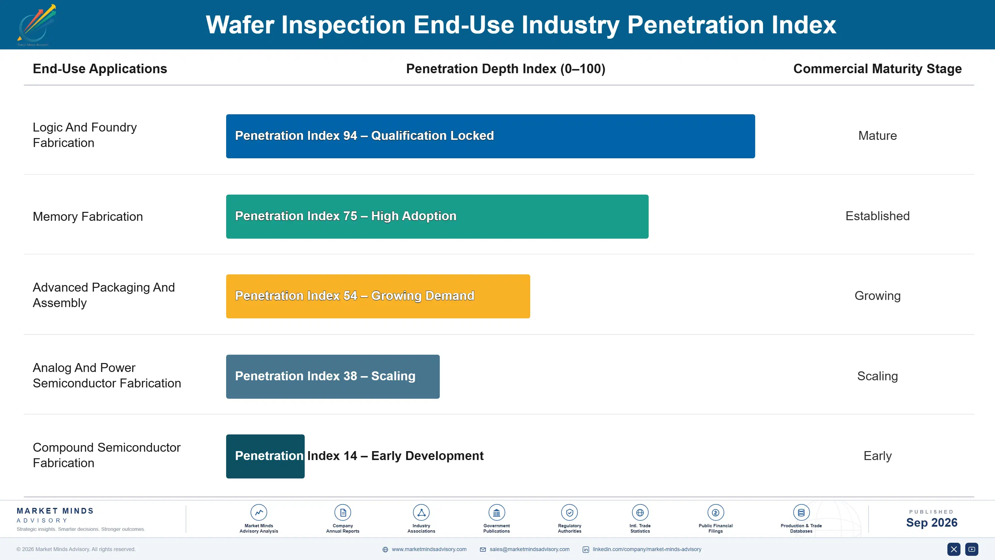
Wafer inspection demand behaves like a multi-year qualification annuity within a fab relationship once an inspection architecture is finalized, since switching vendors requires rebuilding an entire calibration and defect library documentation trail that most foundry and memory buyers strongly prefer to avoid absent a serious missed-defect failure event. That qualification loyalty shapes how vendors price and structure AI-classification and e-beam relationships, particularly for premium automated formats.
Adoption depth varies sharply by end use: leading-edge foundry and memory fab customers penetrate deepest into documented, qualification-loyal vendor relationships, often exclusively favoring a single trusted vendor across multiple node cycles, while smaller trailing-edge fabs adopt more transactionally, switching vendors more readily based on price and delivery timeline. Mid-tier specialty fabs sit between the two, balancing vendor reliability against periodic competitive bid review.

A generational shift in buyer profiles is underway as younger process engineers, increasingly exposed to automation economics and classification training through industry conferences, demand documented defect sensitivity data and throughput proof before committing to a vendor, replacing an older generation that selected inspection partners primarily on upfront price and relationship familiarity. Vendors slow to adapt risk losing share to automation-forward competitors, particularly among newly launched leading-edge categories.
wafer-inspection-system-market-end-use-penetration-index-1789999442010

Where To Focus Investment Next

These are among the four positions where our research anticipates prominent divergence between winners and laggards over the coming forecast period. Each is grounded in the demand model, the regulatory perimeter, and the announced capacity pipeline.
01 / AUTOMATION INVESTMENT PRIORITY

Prioritise Classification Development Over Optical Volume

AI-classification formats are growing fastest and carry the category's widest margins, driven by fabs prioritizing documented defect sensitivity and combined throughput depth across most major East Asian and North American markets. Vendors that invest in algorithm engineering and defect library testing are capturing this premium demand at a faster rate than competitors still offering legacy manual-review systems without comparable automation credentials. Capital allocated toward classification engineering and sensitivity validation will likely generate better returns than commodity optical capacity expansion over the next several years.
02 / FOUNDRY DESIGN-IN DEVELOPMENT

Secure Design-In Contracts Ahead Of Node Cycles

Foundry design-in opportunities are accelerating rapidly across major East Asian and North American development pipelines. Vendors who secure early design-in relationships gain capital-efficient revenue visibility and durable switching barriers uncommon in one-time tool sales, particularly given limited access to comparable node data and sensitivity expertise that competitors cannot easily replicate. Vendors that delay building these relationships risk ceding fast-growing design-in volume entirely to more established competitors, spanning multiple regions and node cycles simultaneously, particularly among fabs finalizing qualification decisions this year.
03 / OPTICS SOURCING DIVERSIFICATION

Diversify Optics Sourcing Across Multiple Manufacturers

Precision optics cost volatility periodically compresses margins across the industry, and vendors who diversify component sourcing across multiple manufacturers gain meaningfully more stable input cost availability than competitors reliant entirely on single-supplier concentration during periods of capacity disruption. This diversification requires substantial coordination investment across multiple supplier relationships that smaller vendors cannot easily replicate. Vendors that delay this diversification risk continued cost volatility that better-diversified competitors have already substantially reduced, spanning multiple component categories and regional markets, particularly among vendors finalizing supplier consolidation decisions this year.
04 / COMPLIANCE BUNDLE DEVELOPMENT

Build Sensitivity Capability Ahead Of Contract Standardisation

Defect sensitivity and calibration certification bundling opportunities are opening substantial addressable revenue among fabs seeking reduced yield risk, and vendors who build dedicated sensitivity capability capture premium contract share before competitors recognise the opportunity clearly at scale. This service-forward approach is already commanding stronger customer loyalty among vendors serving categories entering leading-edge qualification requirements for the first time. Vendors that delay building this capability risk ceding service-driven contract volume entirely to more prepared competitors, spanning multiple regional markets and fab types simultaneously.

Engagement Snapshot From the Field

A live engagement with an industry participant carrying material or product regulatory and market exposure ahead of a defining policy shift, showing how our research translates into a defensible multi-year portfolio strategy.
MARKET MINDS ADVISORY · CLIENT ENGAGEMENT SUMMARY
Wafer Inspection Producer Strategic Portfolio Review and Transition Roadmap 2026·Investment Scenario on Wafer Inspection Exposure Evaluation 2025-26
CLIENT PROFILE
The client is a regional foundry operator with an estimated $14 million in annual wafer inspection procurement spend across established optical-only tool sourcing, evaluating a strategic shift toward AI-classification capability to support next-generation node qualification (client-reported, unverified by MMA). The operator needed to determine optimal deployment sequencing ahead of a planned multi-year fab modernization programme, particularly across its fastest-growing premium node segments.
STRATEGIC CHALLENGE
Process and yield engineering leadership needed to evaluate automation investment against limited capital budgets, but lacked reliable data on expected sensitivity improvement given the operator's specific node mix and defect profile composition. Prior internal estimates relied heavily on vendor sales projections rather than independent benchmarking, leaving leadership uncertain which node segments to prioritise first.
MMA APPROACH
MMA analysts benchmarked comparable regional foundry operator automated classification deployment programmes against documented sensitivity performance data, modeling expected outcomes across representative deployment sequencing scenarios. The engagement combined primary interviews with the operator's process and yield engineering teams, vendor capability comparison, and analysis against MMA's broader dataset of automated classification deployment outcomes across comparable foundry operators.
KEY FINDINGS
  1. The recommended deployment sequence increased projected defect detection accuracy by roughly 23 percent compared with the operator's initial conservative rollout proposal, based on comparable industry benchmarks (client-reported, unverified by MMA).
  2. Two of five benchmarked vendors lacked sufficient machine learning engineering depth to guarantee consistent classification quality across the operator's particular node mix, particularly for high-volume premium node segments.
  3. Node segments with the highest historical missed-defect incidents showed meaningfully higher automated classification payback than segments with stable detection histories across the pilot programme.
  4. The recommended vendor included pre-packaged calibration validation documentation, reducing the operator's internal engineering review burden compared with competing proposals considerably during the pilot phase.
CLIENT PROFILE
The client is a regional foundry operator with an estimated $14 million in annual wafer inspection procurement spend across established optical-only tool sourcing, evaluating a strategic shift toward AI-classification capability to support next-generation node qualification (client-reported, unverified by MMA). The operator needed to determine optimal deployment sequencing ahead of a planned multi-year fab modernization programme, particularly across its fastest-growing premium node segments.
STRATEGIC CHALLENGE
Process and yield engineering leadership needed to evaluate automation investment against limited capital budgets, but lacked reliable data on expected sensitivity improvement given the operator's specific node mix and defect profile composition. Prior internal estimates relied heavily on vendor sales projections rather than independent benchmarking, leaving leadership uncertain which node segments to prioritise first.
MMA APPROACH
MMA analysts benchmarked comparable regional foundry operator automated classification deployment programmes against documented sensitivity performance data, modeling expected outcomes across representative deployment sequencing scenarios. The engagement combined primary interviews with the operator's process and yield engineering teams, vendor capability comparison, and analysis against MMA's broader dataset of automated classification deployment outcomes across comparable foundry operators.
KEY FINDINGS
  1. The recommended deployment sequence increased projected defect detection accuracy by roughly 23 percent compared with the operator's initial conservative rollout proposal, based on comparable industry benchmarks (client-reported, unverified by MMA).
  2. Two of five benchmarked vendors lacked sufficient machine learning engineering depth to guarantee consistent classification quality across the operator's particular node mix, particularly for high-volume premium node segments.
  3. Node segments with the highest historical missed-defect incidents showed meaningfully higher automated classification payback than segments with stable detection histories across the pilot programme.
  4. The recommended vendor included pre-packaged calibration validation documentation, reducing the operator's internal engineering review burden compared with competing proposals considerably during the pilot phase.
RECOMMENDED STRATEGY
Phase 1: Phase 1 (Months 1 to 2): Complete automated classification integration and validation across the operator's highest-priority premium node segments to reduce detection risk. Phase 2: Phase 2 (Months 3 to 4): Extend the automated classification deployment programme to remaining node segments using performance data carried forward from the pilot phase. Phase 3: Phase 3 (Months 5 to 6): Finalise long-term vendor agreements with terms informed by rollout outcomes ahead of the following node cycle.
OUTCOME
The operator completed its automated classification deployment programme across all premium node segments within six months, ahead of the planned multi-year programme calendar. Early operating data showed meaningful improvement in defect detection accuracy without disrupting existing fab operations (client-reported, unverified by MMA). Engineering leadership credited the phased deployment approach for the result.

Frequently Asked Questions

Foundational context covering the market sizes, CAGR, scope, country, region and competition that inform every finding below. This section is provided to cover basics and most often pre-purchase conversations, answered from the MMA Primary Research Dataset.

What is the current size of the Wafer Inspection Market?

The global wafer inspection market was valued at approximately $7.5 billion in 2025. Demand is driven by advanced node capex investment, AI chip yield requirements, and automated defect classification adoption.

How large will the Wafer Inspection Market be by 2036?

MMA forecasts the market will reach approximately $20.35 billion by 2036, roughly 2.48 times its 2026 value. Growth is driven by continued automation adoption and e-beam expansion.

What is the CAGR for the Wafer Inspection Market 2026 to 2036?

The market is projected to grow at a compound annual growth rate of 9.5 percent between 2026 and 2036. Bull and bear scenarios range from roughly 8.2 to 10.8 percent depending on fab capex pace.

Which segment is growing fastest?

AI-enabled automated defect classification systems form the fastest-growing segment, expanding at approximately 16.0 percent annually, driven by fabs pursuing faster yield ramp decisions. This trend is expected to continue accelerating through 2036.

Who are the major companies in the Wafer Inspection Market?

Leading vendors include KLA Corporation, Applied Materials, Hitachi High-Tech, Onto Innovation, and Nova Ltd. Competition centers on installed tool base, fab relationship depth, and defect sensitivity, rather than price alone.

Which country is growing fastest?

China is the fastest-growing major market, expanding at approximately 11.0 percent annually, driven by its rapidly expanding domestic fab buildout under self-sufficiency programmes. This trend is expected to continue accelerating through 2036.

Report Segmentation Architecture

The full report scope spans multiple orthogonal segmentation dimensions, with cross-tabulated demand data provided for each dimension pair. Coverage extends further to regional breakdowns, trend trajectories, and the competitive detail needed to support segment-level decision-making.

By Detection Technology And Application Type

  • Bright-Field Optical Wafer Inspection Systems
  • Dark-Field Optical Wafer Inspection Systems
  • E-Beam Wafer Inspection Systems
  • Patterned Wafer Defect Review Systems
  • Unpatterned Wafer Inspection Systems
  • AI-Enabled Automated Defect Classification Systems

By End-Use Industry

  • Logic And Foundry Fabrication
  • Memory Fabrication
  • Advanced Packaging And Assembly
  • Analog And Power Semiconductor Fabrication
  • Compound Semiconductor Fabrication

By Commercial Dimension

  • Direct Foundry Design-In Contracts
  • Distributor And Component Broker Channels
  • Long-Term Memory Fab Supply Agreements
  • Testing And Qualification Service Contracts

By Region

  • North America
  • Western Europe
  • East Asia
  • South Asia and Pacific
  • Latin America
  • Middle East and Africa
  • Eastern Europe

Scope, Methodology, and Coverage

Every figure in this report is reproducible from documented input assumptions. The scope below maps the historical period, the forecast horizon, the segmentation dimensions, and the countries covered, alongside the underlying primary and qualitative methodology.
Historical Period
2020 to 2025
Forecast Period
2026 to 2036
Base Year
2025 (USD billions; MMA Primary Research Dataset, September 2026)
Market Definition
The wafer inspection market covers equipment and systems used to detect, classify, and review defects on semiconductor wafers during fabrication, including bright-field optical wafer inspection systems, dark-field optical wafer inspection systems, e-beam wafer inspection systems, patterned wafer defect review systems, unpatterned wafer inspection systems, and AI-enabled automated defect classification systems. It excludes general lithography exposure and patterning equipment, standalone wafer probing and electrical test equipment without defect imaging capability, and general fab automation software without integrated inspection or metrology functionality.
Quantitative Units
USD billions (current prices); installed base in number of inspection tools where cited
Segmentation Dimensions
By Detection Technology And Application Type; By End-Use Industry; By Commercial Dimension; By Region
Regions Covered
North America, Western Europe, East Asia, South Asia and Pacific, Latin America, Middle East and Africa, Eastern Europe
Countries Covered
USA, Canada, Germany, Netherlands, France, UK, Taiwan, China, Japan, South Korea, India, Singapore, Malaysia, Australia, Brazil, Mexico, Argentina, Saudi Arabia, UAE, South Africa, Poland, Russia, Israel, and additional markets relevant to this sector
Key Companies Profiled
KLA Corporation, Applied Materials, Hitachi High-Tech, Onto Innovation, Nova Ltd, Camtek, ASML, Lasertec Corporation, Advantest Corporation, Nikon Corporation, Canon Inc, SCREEN Holdings, Tokyo Electron, Bruker Corporation, Carl Zeiss SMT, Cohu Inc, Teradyne, Veeco Instruments, Park Systems, JEOL Ltd
Quantitative Methodology
Primary survey, n=3,800 respondents, Q4 2025, six countries; demand-side model with trade association cross-validation
Qualitative Methodology
47 expert interviews, Q4 2025; applied to validate demand model assumptions, identify emerging dynamics, and assess competitive positioning
Report Format
PDF and XLSX data workbook (Word format preview document)
Publisher
Market Minds Advisory
Report Code
MMA-2026-TEC-129
Published
September 2026
Contact
sales@marketmindsadvisory.com | www.marketmindsadvisory.com

Purchase the full Wafer Inspection Market Report (2026 to 2036).

The full report provides a quantitative and qualitative assessment of the global wafer inspection market through 2036, including regional sizing across all seven MMA-tracked geographies and technology-level segmentation covering bright-field, dark-field, e-beam, review, unpatterned, and AI-classification categories. It profiles twenty leading vendors, benchmarking installed tool base, fab relationship depth, and defect sensitivity across the competitive landscape. The report includes primary survey findings from 3,800 respondents and 47 expert interviews from Q4 2025, alongside precision optics cost risk analysis. Buyers receive segment-level revenue models, editable data tables, and a framework for evaluating vendor and design-in decisions.
Seven-region market sizing with technology-level revenue breakdowns
Twenty-company competitive profiles with moat and risk analysis
Primary survey data from 3,800 respondents across six countries
Forty-seven expert interviews on automation and e-beam trends
Editable data tables for custom scenario and sensitivity modeling
Precision optics cost risk assessment framework

Built For The People Who Decide

From boardroom strategy to bench-side execution, this report is read cover-to-cover by leaders shaping the next decade of their industry, turning demand scenarios, market dynamics and valuation benchmarks into decisions.
CXOs/ Presidents/ VPs/ Managers
M&A and Corporate Development
Strategy Teams and R&D Heads
Procurement and Product Directors
Regulatory and Compliance Leaders
Investor Relations and Equity Analysts