Market Minds Advisory
Thin Wafers Market

Thin Wafers Market: Thin Wafers Market: Breakage Economics, Carrier Bonding Costs and Yield Nobody Discloses 2026 to 2036

Below a certain thickness a silicon wafer stops behaving like a rigid object and starts behaving like paper. Everything expensive in this business follows from handling something that will not stay flat.

Lead Analyst

Published

September 2026

Make Smarter Decisions with Customized Research Insights

Request a free sample report and evaluate market opportunities, growth trends, and competitive dynamics relevant to your business needs.

2025 MARKET VALUE$3.9BMarket Size 2025
2036 FORECAST VALUE$13.5BBase Case , 2026 to 2036
CAGR 2026 TO 203611.9 %Bull 13.2% / Bear 10.6%
INCREMENTAL OPPORTUNITY$9.1BNet 10- year value creation
EXPANSION MULTIPLE3.07x2036 value over 2026 base
Strategic Levers
M&A Pipeline
Regional Outlook
Country Rankings
Competitive Intelligence
Segmental Deep-dive
Call-Us : 91 93563 13602

Executive Snapshot and Market Trajectory.

Below a certain thickness a silicon wafer stops behaving like a rigid object and starts behaving like paper. Everything expensive in this business follows from having to handle something that will not stay flat on its own. Around 4% of wafers break at aggressive thickness targets.
The market reaches USD 4.4 billion in 2026 and USD 13.5 billion by 2036, a 3.07 times expansion at 11.9% annually. Sub-50 micron wafers for stacked memory grow at 17.9%, half again the market rate of 11.9%, because stacking dies is the only route left to memory bandwidth. East Asia holds 52% of processing value, far above the usual band, on packaging concentration. Yield decides purchases here.
Five participants hold 71% of thinning and handling value, very high and reflecting equipment installed base rather than any process advantage. Disco Corporation, Tokyo Electron, Applied Materials, EV Group and Brewer Science lead. Breakage rate at target thickness decides most competitive outcomes here. Temporary bonding and debonding absorb around 29% of processing cost and generate most of the breakage, which makes that step a larger commercial position than the grinding everybody watches.
Market Definition
This report covers thin wafer processing: the equipment, materials and services that reduce semiconductor wafers below conventional thickness and handle them through subsequent process steps. It spans sub-50 micron wafers for stacked memory, temporary carrier bonding and debonding materials and equipment, wafer grinding and thinning equipment, thin wafer handling and transport systems, taping and dicing consumables for thinned wafers, and metrology for thickness and stress measurement. It excludes bulk wafer manufacturing, front end lithography and deposition equipment, packaging substrates, die attach materials, and finished packaged devices.
Base Year Value
$3.9B in 2025 (MMA Primary Research Dataset, September 2026)
Forecast Period
2026 to 2036, eleven discrete annual values
CAGR
11.9% base case. Bull 13.2%. Bear 10.6%.
Fastest Growth Segment
Sub-50 Micron Wafers For Stacked Memory: 17.9% CAGR
Fastest Growth Country
India: 19.3% CAGR
Fastest Growth Region
South Asia and Pacific: 14.2% CAGR
Largest Region
East Asia: 52% of 2025 global value
Market Leaders
Disco Corporation, Tokyo Electron, Applied Materials, EV Group and Brewer Science lead on thin wafer processing equipment and materials revenue. Source: MMA Analysis.
Primary Survey
n=3,800 procurement and R&D decision-makers, Q4 2025, six countries
Methodology
Demand-side build-up, cross-validated against public data, 47 expert interviews

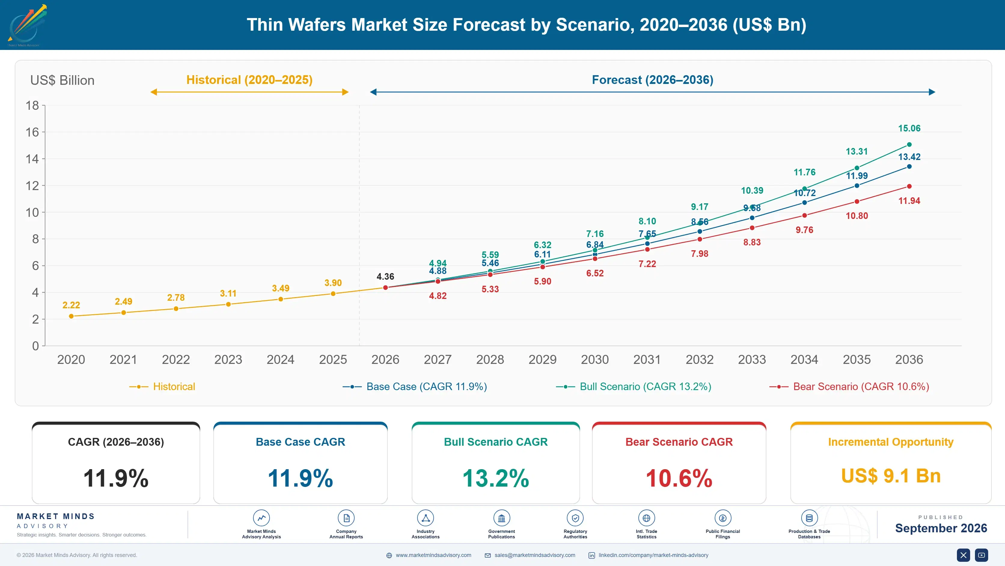
Thin Wafers Market Forecast Scenarios

thin-wafers-market-size-forecast-scenario-1790002932683
Between 2020 and 2025 the category compounded at 10.5%, and the driver moved from power devices to memory stacking. Thinning had been a niche requirement for power semiconductors and image sensors for years. Stacked memory changed that: the only remaining route to bandwidth is putting dies on top of each other, and that requires wafers thin enough to stack without the package becoming impossibly tall.
The base case holds 11.9% on three mechanisms. Stacked memory demand keeps rising because bandwidth cannot be improved any other way at acceptable power. Advanced packaging keeps moving logic toward chiplet architectures that require thinned dies to interconnect vertically. And power device manufacturers keep thinning further to reduce conduction losses, which is a separate driver operating on entirely different economics from either of the others. Those three mechanisms run largely independently of one another.
The bull case at 13.2% assumes stacked memory layer counts keep rising as planned, since each additional layer requires thinner wafers still and compounds handling difficulty. The bear case at 10.6% is yield discipline, where breakage at target thickness stays high enough that memory manufacturers slow layer count increases rather than absorbing the loss that aggressive thinning produces.

Silicon That Behaves Like Paper

A wafer at 40 microns is thinner than most paper and behaves accordingly. It bows, it cracks under its own handling and it cannot be moved through a fab without a carrier holding it flat. Around 4% of wafers are lost during thinning and handling at aggressive targets, and that figure sits on top of everything already invested in the wafer before it reached this step at all.
TOP FIVE CONCENTRATION71%Very high, reflecting installed equipment base rather than process advantage
TARGET WAFER THICKNESS40 micronsTypical thickness for wafers destined for stacked memory assembly
BREAKAGE RATE AT TARGET4%Wafers lost during thinning and handling at aggressive thickness targets
CARRIER BONDING COST SHARE29%Temporary bonding and debonding within total thin wafer processing cost
EQUIPMENT SERVICE LIFE11 yearsTypical working life of installed grinding and bonding equipment
MEMORY APPLICATION SHARE46%Processing volume driven by stacked memory rather than power devices
Temporary bonding is where the cost actually concentrates. Attaching a wafer to a rigid carrier and then removing it without damage absorbs around 29% of thin wafer processing cost, and the debonding step is where most breakage happens. That makes bonding materials and debonding equipment a considerably larger commercial position than the grinding that gets all the attention, and it explains why materials companies sit among the leaders.
Memory stacking displaced power devices as the volume driver. Around 46% of processing volume now serves stacked memory rather than power semiconductors, because stacking dies is the only remaining route to bandwidth at acceptable power. Sub-50 micron wafers for stacked memory grow at 17.9% against 11.9% for the market, and each additional stack layer requires thinner wafers than the one before it.
"Everyone focuses on the grinder because it is the visible machine. The money and the yield loss are both in bonding the wafer to a carrier and getting it off again intact. I have seen fabs with excellent grinding lose four percent of production at debond and call it a materials problem."
Director, Semiconductor Packaging and Wafer Processing Practice · MMA Technology Practice · September 2026

Market Trends

Memory Stacking Replaced Power Devices As Driver

Around 46% of thin wafer processing volume now serves stacked memory rather than power semiconductors, because stacking dies vertically is the only remaining route to bandwidth at acceptable power consumption. Sub-50 micron wafers for stacked memory grow at 17.9% against 11.9% for the market, and every additional stack layer requires thinner wafers than the layer before it. That compounding requirement is what makes this the fastest moving part of semiconductor packaging. Layer count roadmaps are published years ahead and translate directly into thickness requirements that determine which equipment can even compete for a process.
Market Impact: India compounds at 19.3% yearly
Bonding And Debonding Carry The Cost And Loss

Temporary bonding to a rigid carrier and subsequent debonding absorb around 29% of thin wafer processing cost, and debonding is where most of the roughly 4% breakage actually occurs. That makes bonding materials and debonding equipment a larger commercial position than the grinding step everybody focuses on, which is why materials companies appear among the leaders. Fabs with excellent grinding still lose wafers at debond and frequently misattribute the loss entirely. Single-party responsibility for the whole sequence removes an attribution argument that separate purchasing reliably produces after any loss. Attribution wastes time.
Market Impact: Targets now reach 40 microns

Market Opportunities and Growth Drivers

Chiplet Architectures Require Vertically Interconnected Dies

Logic designs moving toward chiplet architectures need thinned dies to interconnect vertically through the wafer rather than around it, which extends thin wafer demand beyond memory into processor packaging. That requirement grows with the number of chiplets in a package rather than with unit shipments. India compounds at 19.3% partly on packaging capacity being built for exactly these architectures rather than converted from older assembly work. Capacity built for these architectures avoids the retrofit constraints that mature packaging sites face when adding thin wafer capability to an existing process flow.
Market Impact: Breakage runs near 4% today

Power Devices Thin Further To Cut Conduction Losses

Power semiconductor manufacturers keep thinning substrates further because conduction losses fall with thickness, and electrification applications make every percentage point of efficiency commercially material. That driver operates on entirely different economics from memory, since power devices tolerate thicknesses memory stacking cannot use. It also sustains demand for equipment and materials optimised for different thickness ranges, which broadens the addressable requirement rather than concentrating it. Qualification cycles here run on different timescales from memory too, which means a supplier serving both smooths a cycle that otherwise dominates this equipment business entirely.
Market Impact: Bonding carries 29% of cost

Market Restraints and Challenges

Breakage Loss Compounds Everything Already Invested

Around 4% of wafers break during thinning and handling at aggressive targets, and that loss falls on wafers carrying the full value of every process step already completed. The root cause is that silicon below fifty microns has no useful rigidity and stresses concentrate at any handling contact. Commercially this makes yield the deciding purchase criterion. Mitigation runs through carrier bonding chemistry, through handling automation that eliminates contact, and through stress metrology catching problems before debond. Yield rather than throughput is consequently the criterion these fabs purchase against. Throughput barely features.
Market Impact: Memory drives 46% of volume

Debond Failures Get Attributed To The Wrong Step

Most breakage happens at debonding rather than during grinding, yet fabs frequently attribute the loss to whichever supplier is most visible in the process. The root cause is that bonding chemistry, carrier flatness and debond method interact in ways no single supplier controls entirely. Commercially this distorts purchasing decisions. Mitigation runs through integrated bonding and debonding supply from one participant, through joint qualification programmes, and through metrology that identifies where stress originated. The argument itself consumes engineering time that no packaging operation has spare to give. Nobody wins that argument.
Market Impact: Bonding absorbs 29% of cost
3 additional market trends, 4 additional growth drivers, and 2 additional restraints and challenges are covered in the full report. Contact sales@marketmindsadvisory.com to access the complete intelligence.

Segment CAGR and Growth Architecture

Segmentation follows process step and material class, since each carries quite different yield exposure, equipment intensity and buyer within a fab. Six classes cover the market: sub-50 micron wafers for stacked memory, temporary carrier bonding and debonding materials and equipment, wafer grinding and thinning equipment, thin wafer handling and transport systems, taping and dicing consumables, and thickness and stress metrology.
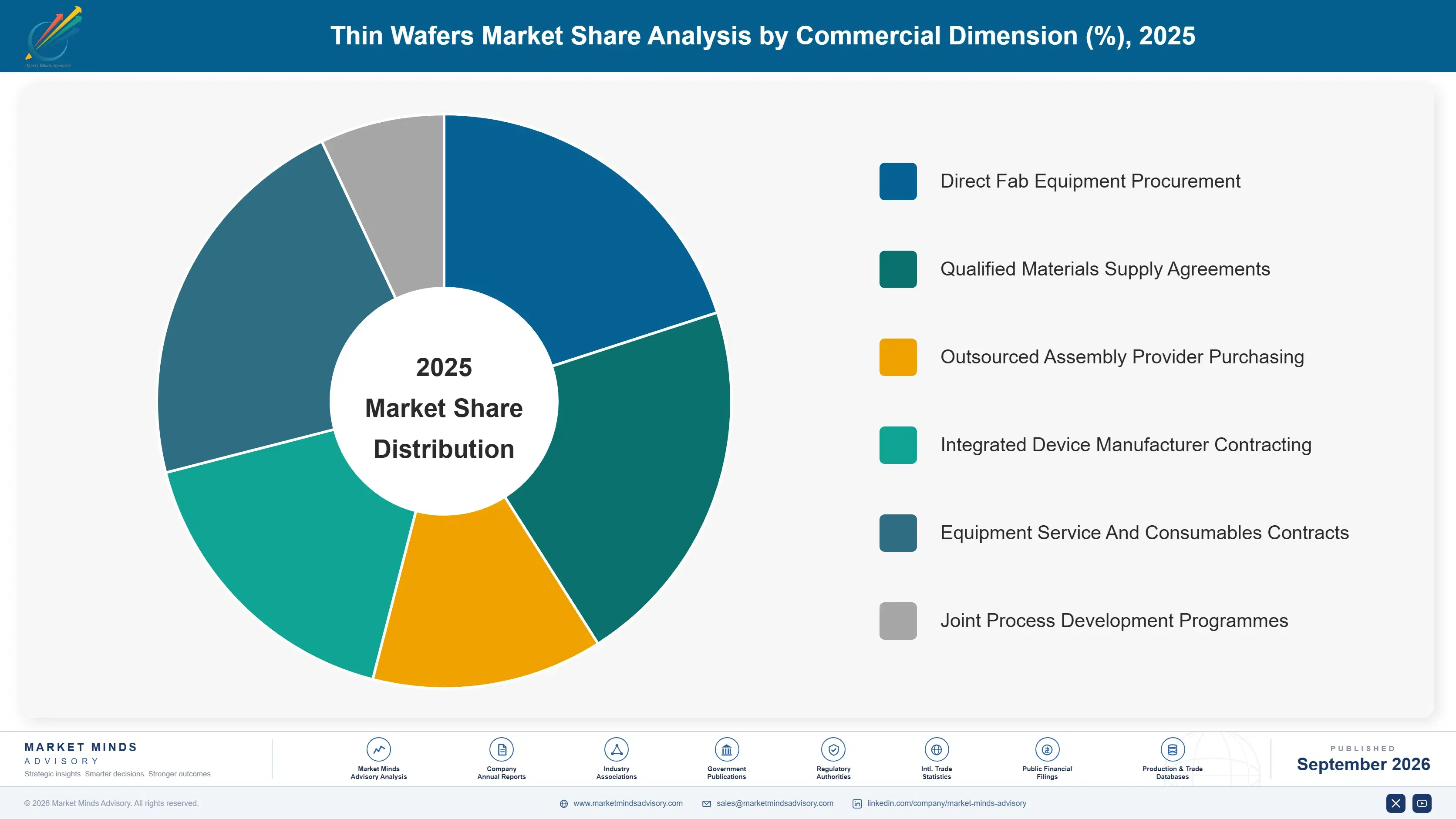
thin-wafers-market-market-share-analysis-1790002933242

Sub-50 Micron Wafers For Stacked Memory

Sub-50 micron wafers for stacked memory grow at 17.9%, half again the market rate of 11.9%, because stacking dies vertically is the only remaining route to memory bandwidth at acceptable power and every additional layer requires thinner wafers than the one below it. Around 46% of processing volume already serves memory rather than power devices. Breakage near 4% at these targets falls on wafers carrying full accumulated process value, which makes yield rather than throughput the criterion memory manufacturers actually purchase against. Layer count roadmaps published years ahead translate directly into thickness targets, which makes demand here forecastable in a way wafer start volumes never were. Forecasting improves accordingly. Wafer starts told nobody anything.
CAGR 17.9%

Temporary Carrier Bonding And Debonding

Temporary carrier bonding and debonding compounds at 15.4% because it absorbs around 29% of thin wafer processing cost and is where most of the roughly 4% breakage actually occurs, which makes it the step that determines whether a thinning process works commercially. Bonding chemistry, carrier flatness and debond method interact in ways no single supplier controls, so integrated supply from one participant carries genuine value. That interaction is also why fabs frequently misattribute losses to the most visible supplier rather than the responsible step. Integrated supply from one participant carries genuine commercial value for exactly that reason. Fabs increasingly want one participant carrying responsibility for the whole sequence rather than two arguing about a loss afterwards.
CAGR 15.4%
Full segment breakdown across 6 segments available in the complete report.

Regional Architecture and Country Demand Map

East Asia holds 52% of thin wafer processing value, far above the usual band, because advanced packaging and memory assembly capacity concentrate there to a degree no other semiconductor activity matches. North America follows at 18% on equipment and materials development. India compounds fastest at 19.3% on new packaging capacity.

East Asia

East Asia takes 52% of thin wafer processing value, far above the 30% band ceiling, because advanced packaging and memory assembly capacity concentrate here to a degree no other semiconductor activity approaches at all. Korean and Taiwanese memory and packaging operations consume the majority of sub-50 micron capacity worldwide, and Disco Corporation and Tokyo Electron both supply from within the region. Japanese materials suppliers hold bonding chemistry positions built across decades. Growth at 12.7% runs above the market rate on stacked memory volume. Bonding chemistry qualification held by Japanese suppliers is among the most durable competitive positions anywhere in semiconductor materials. Displacement is correspondingly rare. Positions turn over slowly. Incumbency holds firmly.
Share: 52% | CAGR: 12.7% (2026 to 2036)

North America

North America accounts for 18% of processing value through equipment development, bonding materials chemistry and the advanced packaging capacity now being built domestically under industrial policy programmes. Applied Materials and Brewer Science both develop from here, and chiplet architectures originating in the region drive requirements that packaging elsewhere then implements. Growth at 12.4% sits above the market rate on domestic packaging capacity addition rather than on any established processing volume within the region. Chiplet architectures defined here set thinning requirements that packaging operations elsewhere then have to implement, which is influence the processing share does not capture. Domestic capacity is being added under industrial policy programmes. Requirements originate here. Implementation happens elsewhere.
Share: 18% | CAGR: 12.4% (2026 to 2036)
Regional intelligence for 5 additional markets available in the complete report: South Asia and Pacific, Western Europe, Eastern Europe, Middle East and Africa, Latin America. Contact sales@marketmindsadvisory.com.
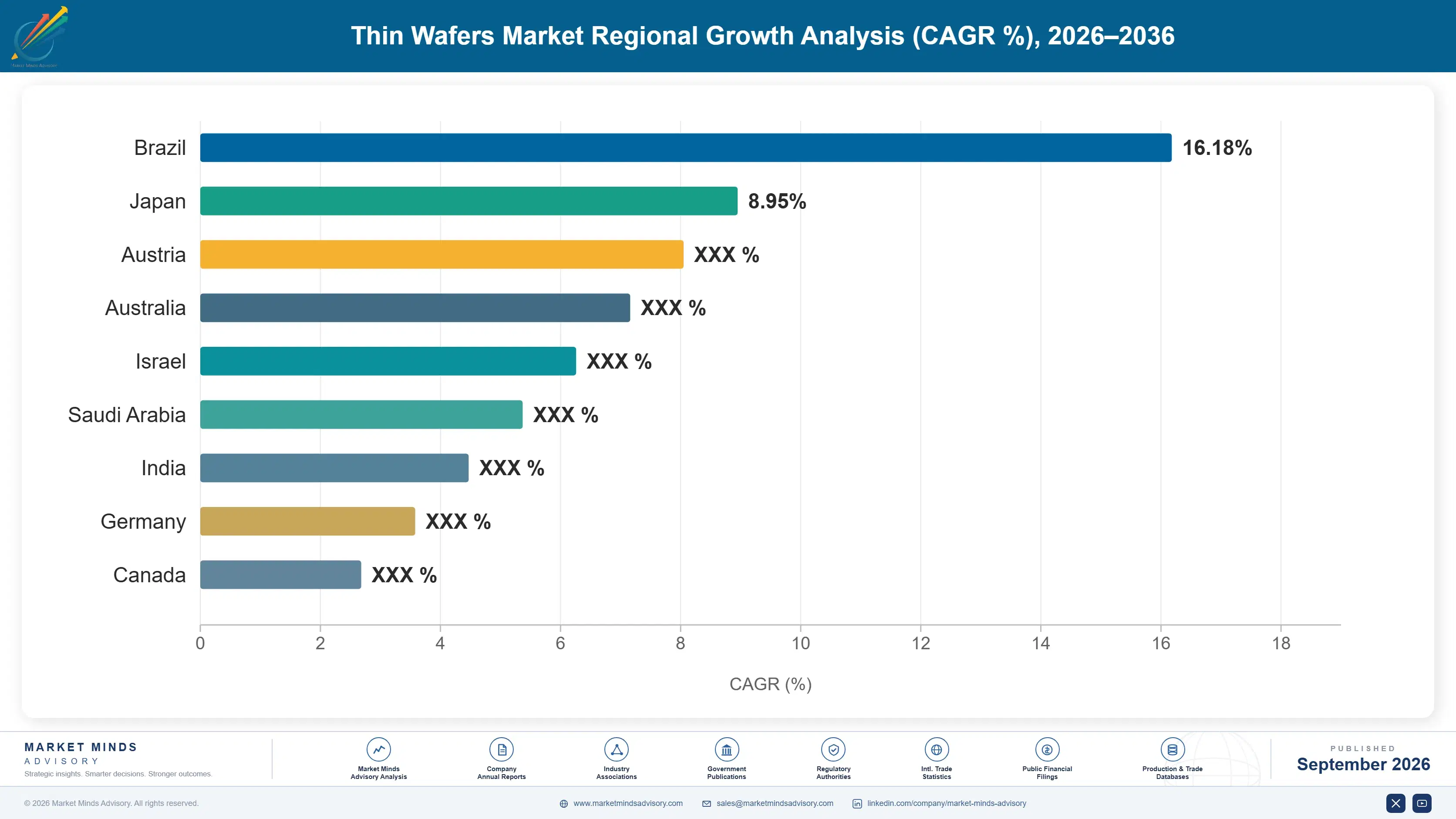
thin-wafers-market-country-cagr-analysis-1790002933800

Where Thinning Value Actually Concentrates

Breakage rather than throughput is what fabs purchase against, bonding and debonding carry the cost and the loss, and memory stacking replaced power devices as the volume driver. The four levers below follow those conditions rather than any argument about grinding capability, which converged years ago. Each addresses a yield condition instead. Grinding converged years ago.

Sell Yield At Target Thickness, Not Throughput

Around 4% of wafers break during thinning and handling at aggressive targets, and that loss falls on wafers carrying the full value of every process step already completed before thinning began. A fab losing 4% of finished-value wafers cares considerably less about throughput than about that number. Suppliers quoting wafers per hour are answering a question memory manufacturers stopped asking once thickness targets reached 40 microns. Accumulated process value is what makes each broken wafer expensive rather than merely wasteful. Throughput answers a different question. Forty micron targets settled it.
Market Impact: Breakage now runs near 4% at target thickness

Supply Bonding And Debonding As One System

Bonding and debonding absorb around 29% of processing cost and most of the roughly 4% breakage occurs at debond, yet bonding chemistry, carrier flatness and debond method interact in ways no single supplier controls when they are bought separately. Integrated supply from one participant removes the interaction problem and the attribution argument that follows a loss. That is worth more to a fab than any individual component advantage anybody can demonstrate. Engineering time spent arguing is time nobody has. Component advantage matters less than sequence ownership. Fabs increasingly insist on it.
Market Impact: Bonding now absorbs 29% of all processing cost

Follow Layer Counts Rather Than Wafer Starts

Around 46% of processing volume serves stacked memory, and demand there grows with stack layer count rather than with wafer starts, since each additional layer requires thinner wafers than the one below. Suppliers forecasting from wafer volumes are modelling the wrong variable for the fastest growing application. Layer count roadmaps are published years ahead and translate directly into thickness requirements that determine which equipment can even compete. Wafer start forecasts miss it entirely. Roadmaps publish thickness requirements years ahead, which makes this the one forecastable demand signal in the whole category.
Market Impact: Memory now drives fully 46% of all volume

Serve Power Device Thickness Ranges Separately

Power semiconductor manufacturers thin substrates to cut conduction losses at thicknesses memory stacking cannot use, which is a genuinely separate requirement operating on different economics and different qualification cycles. Suppliers optimising exclusively for 40 micron memory targets forgo a demand stream that grows with electrification rather than with bandwidth. Serving both broadens the addressable requirement and smooths the memory cycle that otherwise dominates this equipment business entirely. Electrification rather than bandwidth drives that demand. Qualification cycles differ too, which spreads risk across two application bases that rarely turn down together.
Market Impact: Targets now reach 40 microns for stacked memory

Who Controls the Margin Pool

Five participants hold 71% of thin wafer processing value, very high even for semiconductor equipment, and that position reflects installed equipment base and qualified materials rather than any process advantage anybody currently holds. Disco Corporation, Tokyo Electron, Applied Materials, EV Group and Brewer Science lead. All participants are assessed on thin wafer processing equipment and materials revenue rather than on broader semiconductor equipment or chemicals businesses. Concentration has held because equipment lasting around eleven years turns positions over very slowly indeed.
Competition runs on demonstrated yield at target thickness and on qualification position far more than on equipment specification, which converges quickly. The second dimension is integrated bonding and debonding supply, because those steps interact in ways separate suppliers cannot control and fabs increasingly prefer one participant carrying responsibility for the whole sequence. Equipment specification competes a distant third.

Pressure is emerging from memory manufacturers developing internal thinning process capability, which reduces equipment supplier influence over process definition. Rankings shift where packaging capacity is built and where stack layer counts rise, particularly across Korea, Taiwan and India over the coming decade. Suppliers holding only one step in the bonding sequence carry the most exposure to that preference.
thin-wafers-market-company-positioning-matrix-1790002934332

Competitive Moat and Risk Dimensions

DISCO CORPORATION

Moat: Grinding Installed Base

Disco holds an installed grinding and dicing base across packaging operations worldwide that took decades to establish, and equipment lasting around eleven years means those positions turn over slowly. Process recipes developed on that equipment carry accumulated yield learning a competitor cannot transfer. Fabs changing grinding supplier restart process qualification on wafers carrying full accumulated value, which they rarely accept.
DISCO CORPORATION

Risk: Bonding Step Absence

Bonding and debonding absorb around 29% of processing cost and generate most of the roughly 4% breakage, which is where fabs increasingly want integrated responsibility from a single supplier. Grinding position does not extend into that sequence. A participant strong in the visible step and absent from the expensive one cedes the integration argument to competitors offering both.
BREWER SCIENCE

Moat: Bonding Chemistry Depth

Brewer Science holds temporary bonding chemistry qualified across memory and logic packaging processes, and that qualification takes years because failures appear at debond rather than at bonding. Around 29% of processing cost sits in this step. Competitors with comparable chemistry and no qualification history cannot be evaluated without a fab risking wafers carrying full accumulated process value.
BREWER SCIENCE

Risk: Equipment Integration Gap

Bonding chemistry works only in combination with debonding equipment and carrier handling that the company does not supply, which leaves the integration argument to participants offering both together. Fabs increasingly want single-party responsibility for the whole sequence. Materials depth without equipment leaves the supplier exposed whenever an integrated competitor qualifies successfully.

Players Tracked

Prominent Players

Disco Corporation
Tokyo Electron
Applied Materials
EV Group
Brewer Science

Other Key Players

SUSS MicroTec
Lam Research
Tokyo Ohka Kogyo
Shin-Etsu Chemical
Nitto Denko
Okamoto Machine Tool
Revasum
Lintec Corporation
Hamamatsu Photonics
Onto Innovation
KLA Corporation
G and N Genauigkeits Maschinenbau
Ultratech Stepper
Toray Engineering
JSR Corporation

Recent Developments

MARCH 2025

Memory Manufacturers Raise Stack Layer Count Targets

Memory manufacturers raised stacked die layer count targets, a product roadmap development rather than any corporate transaction. Each additional layer requires thinner wafers than the one below it, which compounds handling difficulty and pushes thickness targets below levels where breakage near 4% is already the deciding purchase criterion for equipment.
Signal: Layer count roadmaps now translate directly into thickness requirements determining which equipment can even compete anywhere.
SEPTEMBER 2024

Fabs Seek Integrated Bonding And Debonding Responsibility

Packaging operations increasingly sought bonding materials and debonding equipment from a single supplier, a procurement development rather than any acquisition. Bonding chemistry, carrier flatness and debond method interact in ways separate suppliers cannot control, and the attribution argument after a loss consumes engineering time nobody has.
Signal: Single-party responsibility removes an attribution argument that separate supply arrangements now reliably produce after every loss.
JUNE 2025

Indian Packaging Capacity Specifies For Chiplet Architectures

Indian packaging capacity under construction specified equipment for chiplet and stacked architectures rather than conventional assembly, a specification development rather than any corporate event. India compounds at 19.3%, and capacity built for these architectures avoids the retrofit constraints that mature packaging sites face when adding thin wafer capability.
Signal: New capacity specifies at design stage where mature sites must retrofit around their existing process flows.

What Thinning Costs

Bonding and debonding materials absorb roughly 29% of thin wafer processing cost, sourced from a small group of specialist chemistry suppliers whose formulations are qualified per process. Equipment depreciation takes around 24% across grinding, bonding and handling tools. Yield loss absorbs about 19% at aggressive thickness targets, and consumables including grinding wheels and tapes take the remaining balance.
Specialty chemistry input costs rose through 2023 and 2024 as advanced packaging demand outpaced the specialist supply base producing qualified bonding formulations. Tokyo Ohka Kogyo Annual Report 2024 and Disco Corporation Annual Report 2024 both record materials availability and qualification cost among principal operating variables. Fabs holding multi-year materials agreements avoided requalification that a supply interruption would otherwise have forced on them. Requalification takes months nobody plans for.

The competitive disadvantage mechanism is yield loss rather than materials price. A fab losing 4% of wafers at debond carries a cost far exceeding any materials saving available, because those wafers carry full accumulated process value from every earlier step. Exposure concentrates among operations buying bonding materials and debonding equipment separately, since the interaction between them is where losses originate and neither supplier owns the outcome.
thin-wafers-market-cost-volatility-analysis-1790002934531

Buy Bonding Materials And Debonding Equipment Together

Bonding and debonding absorb around 29% of processing cost and generate most of the roughly 4% breakage, and the interaction between chemistry, carrier and debond method is where losses originate. Single-party supply puts responsibility for that interaction with one participant. It also removes the attribution argument after a loss, which consumes engineering time that no packaging operation has spare.

Deploy Stress Metrology Before The Debond Step

Yield loss absorbs about 19% of processing cost at aggressive targets and most of it appears at debond, by which point the wafer carries full accumulated process value. Stress measurement before debonding identifies wafers likely to fail while intervention is still possible. The metrology cost is small against the value of a wafer that has completed every prior step.

Qualify Alternative Bonding Chemistry Ahead Of Need

Bonding formulations come from a small specialist supply base and are qualified per process, which makes a supply interruption a requalification event rather than a purchasing inconvenience. Qualifying an alternative before it is needed preserves production continuity. The work takes months and has no value unless it was completed well before the interruption that makes it necessary.

Portfolio Architecture for Margin Defence

Margin architecture separates on yield responsibility rather than on equipment sophistication. Taping and dicing consumables earn least, since they are recurring supplies competing on price with several qualified alternatives available. Grinding equipment and handling systems sit above on installed base and process recipe attachment. Bonding and debonding, sub-50 micron processing and stress metrology earn most, because each carries direct responsibility for the yield fabs actually purchase against.
The volume versus premium tension runs between consumables and integrated process responsibility, which reward opposite commercial positions entirely. Consumables generate recurring revenue at modest margin across every wafer processed. Integrated responsibility commands far more and carries the risk of being blamed when yield falls. Suppliers avoiding that responsibility keep the safer revenue and concede the position fabs increasingly want somebody to occupy.

High-value pools concentrate in bonding and debonding and in sub-50 micron capability, and neither is reached through equipment engineering alone. Bonding requires chemistry qualified per process across years of failure data. Sub-50 micron requires handling that eliminates contact entirely. Both explain why five participants hold 71% while the consumables half of this market supports several additional suppliers competing on price.

Volume / Commodity-Adjacent

Taping and dicing consumables for thinned wafers, recurring supplies competing on price where several qualified alternatives exist for most processes. The twelve point spread separates suppliers with qualified positions across many processes from those serving a narrow set of fabs.
Gross Margin: 27% to 39%

Premium / Certified

Wafer grinding and thinning equipment and thin wafer handling and transport systems, where installed base and accumulated process recipes determine selection more than specification does. The thirteen point spread tracks how much process learning each supplier has embedded across customer operations.
Gross Margin: 44% to 57%

Sustainability / Regulatory / Next-Generation

Temporary bonding and debonding, sub-50 micron processing capability and thickness and stress metrology, each carrying direct responsibility for the yield fabs purchase against. The seventeen point spread reflects qualification depth and whether a supplier owns the whole bonding sequence.
Gross Margin: 61% to 78%
thin-wafers-market-portfolio-architecture-1790002935042

High-value Sub-segments and Strategic Watch-out

Sub-50 Micron Wafers For Stacked Memory

Grows at 17.9% because stacking dies vertically is the only remaining route to memory bandwidth at acceptable power. The seventeen point spread reflects handling capability. Each additional stack layer requires thinner wafers than the layer below it. Handling contact is what has to disappear. Contact is the enemy.
Gross Margin: 61% to 78%

Temporary Carrier Bonding And Debonding

Grows at 15.4% because it absorbs around 29% of processing cost and generates most of the breakage that occurs. The seventeen point spread reflects qualification depth. Integrated supply removes an attribution argument that separate purchasing reliably produces. Chemistry and equipment interact constantly. Ownership beats components.
Gross Margin: 61% to 78%

Wafer Grinding And Thinning Equipment

Grows at 10.2% on capacity additions and replacement across an installed base lasting around eleven years. The thirteen point spread reflects embedded process recipes. Changing supplier restarts qualification on wafers carrying full accumulated value. Process recipes carry accumulated yield learning that transfers to nobody. Requalification is refused.
Gross Margin: 44% to 57%

Taping And Dicing Consumables

Grows at 8.1%, slowest of the six classes, as recurring supplies competing on price against several qualified alternatives per process. The twelve point spread reflects qualification breadth. Volume follows wafer processing rather than driving any demand independently. Alternatives are qualified per process. Price decides these awards.
Gross Margin: 27% to 39%

Why Qualification Holds Fabs

The annuity here is process qualification rather than any equipment contract. A bonding chemistry or grinding recipe qualified for a fab's process runs for years, because changing it means risking wafers that carry full accumulated value from every prior step. Around 4% already break at target thickness without anybody changing anything. Fabs decline requalification almost every time it is proposed, which makes incumbency unusually durable across this whole category.
Depth varies by how many steps a supplier owns. A participant supplying bonding chemistry alone carries responsibility for outcomes that also depend on carrier flatness and debond method it does not control. A participant supplying the whole sequence owns the yield and gets credited or blamed accordingly. Fabs increasingly prefer the second arrangement, because the attribution argument after a loss consumes engineering time nobody has.

The buyer has changed as the application moved. A power device process engineer evaluated grinding throughput and surface quality against established thickness targets. A memory packaging engineer evaluates breakage at 40 microns against wafers carrying full process value. A packaging architect evaluates whether the process supports the layer count the roadmap demands. Throughput questions barely feature in the last two conversations at all.
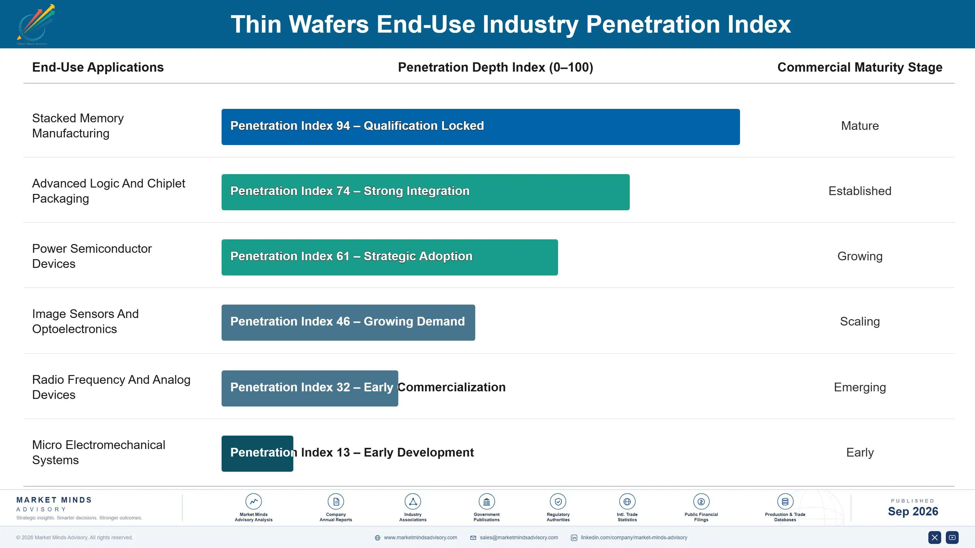
thin-wafers-market-end-use-penetration-index-1790002935562

What Wins Thinning Business

These are among the four positions where our research anticipates prominent divergence between winners and laggards over the coming forecast period. Each is grounded in the demand model, the regulatory perimeter, and the announced capacity pipeline.
01 / YIELD ARGUMENT PRIORITY

Quote Breakage, Not Wafers Per Hour

Around 4% of wafers break during thinning and handling at aggressive targets, and that loss falls on wafers carrying the full accumulated value of every process step completed before thinning ever began. A fab losing finished-value wafers at that rate cares considerably less about throughput than about the breakage number itself. Suppliers quoting wafers per hour are answering a question memory manufacturers stopped asking once thickness targets reached forty microns some years ago now and rarely ask now in any evaluation.
02 / SEQUENCE OWNERSHIP STRATEGY

Own The Whole Bonding Sequence

Bonding and debonding absorb around 29% of processing cost and generate most of the breakage, yet chemistry, carrier flatness and debond method interact in ways no separate supplier controls when bought individually. Integrated supply from one participant removes both the interaction problem and the attribution argument that reliably follows any yield loss. That is worth considerably more to a packaging operation than any individual component advantage a competitor can demonstrate in an evaluation of individual components or supplier claims made in isolation.
03 / ROADMAP DEMAND MODELLING

Forecast Layers, Not Wafer Starts

Around 46% of processing volume serves stacked memory where demand grows with layer count rather than with wafer starts, since each additional layer requires thinner wafers than the one below it. Suppliers forecasting from wafer volumes are modelling entirely the wrong variable for the fastest growing application in this category. Layer count roadmaps are published years ahead and translate directly into thickness requirements determining which equipment can compete for the coming generations and which cannot at each thickness step the roadmap sets.
04 / APPLICATION RANGE BREADTH

Serve Power Devices Alongside Memory

Power semiconductor manufacturers thin substrates to cut conduction losses at thicknesses stacked memory cannot use, which is a genuinely separate requirement running on different economics and qualification cycles entirely. Suppliers optimising exclusively for forty micron memory targets forgo demand that grows with electrification rather than with bandwidth requirements. Serving both broadens the addressable requirement and smooths a memory cycle that otherwise dominates this equipment business completely through every downturn and every memory downturn the industry produces every few years without any warning.

Engagement Snapshot From the Field

A live engagement with an industry participant carrying material or product regulatory and market exposure ahead of a defining policy shift, showing how our research translates into a defensible multi-year portfolio strategy.
MARKET MINDS ADVISORY · CLIENT ENGAGEMENT SUMMARY
Thin Wafers Producer Strategic Portfolio Review and Transition Roadmap 2026·Investment Scenario on Thin Wafers Exposure Evaluation 2025-26
CLIENT PROFILE
An advanced packaging operation losing wafers at rates above its target while running well-regarded grinding equipment, and attributing the loss to grinding performance. Management had approved a grinding equipment replacement programme, without anybody establishing at which process step the breakage was actually occurring across the line. Nobody had instrumented the line to find where breakage originated across the process.
STRATEGIC CHALLENGE
Process engineering wanted new grinding equipment to address the yield problem. Procurement wanted the capital deferred given the cost involved. Nobody had instrumented the line to identify where breakage originated, and the equipment order was scheduled for approval within the quarter on the strength of an assumption. The whole case rested on an untested assumption.
MMA APPROACH
MMA instrumented the process line to identify where wafers were actually failing, measuring stress before and after each step rather than counting losses at the end. We compared bonding chemistry, carrier flatness and debond method against the failure locations found. Work drew on 47 expert interviews conducted in Q4 2025 with packaging operations, equipment suppliers and materials specialists.
KEY FINDINGS
  1. Around 79% of wafer losses occurred at the debond step rather than during grinding, which the replacement programme would not have addressed at all.
  2. Carrier flatness variation from 1 supplier accounted for most of the debond failures, and nobody had been measuring it as an incoming parameter.
  3. Bonding materials and debonding equipment came from separate suppliers, and each attributed the losses to the other repeatedly (client-reported, unverified by MMA).
  4. Stress metrology applied before the debond step identified failure-prone wafers early enough that intervention remained genuinely possible on most of them each time.
CLIENT PROFILE
An advanced packaging operation losing wafers at rates above its target while running well-regarded grinding equipment, and attributing the loss to grinding performance. Management had approved a grinding equipment replacement programme, without anybody establishing at which process step the breakage was actually occurring across the line. Nobody had instrumented the line to find where breakage originated across the process.
STRATEGIC CHALLENGE
Process engineering wanted new grinding equipment to address the yield problem. Procurement wanted the capital deferred given the cost involved. Nobody had instrumented the line to identify where breakage originated, and the equipment order was scheduled for approval within the quarter on the strength of an assumption. The whole case rested on an untested assumption.
MMA APPROACH
MMA instrumented the process line to identify where wafers were actually failing, measuring stress before and after each step rather than counting losses at the end. We compared bonding chemistry, carrier flatness and debond method against the failure locations found. Work drew on 47 expert interviews conducted in Q4 2025 with packaging operations, equipment suppliers and materials specialists.
KEY FINDINGS
  1. Around 79% of wafer losses occurred at the debond step rather than during grinding, which the replacement programme would not have addressed at all.
  2. Carrier flatness variation from 1 supplier accounted for most of the debond failures, and nobody had been measuring it as an incoming parameter.
  3. Bonding materials and debonding equipment came from separate suppliers, and each attributed the losses to the other repeatedly (client-reported, unverified by MMA).
  4. Stress metrology applied before the debond step identified failure-prone wafers early enough that intervention remained genuinely possible on most of them each time.
RECOMMENDED STRATEGY
Phase 1: Phase one: cancel the grinding equipment replacement, since roughly 79% of losses occurred at debond rather than during the grinding step. Phase 2: Phase two: source bonding materials and debonding equipment from one single supplier carrying full responsibility for the entire sequence together. Phase 3: Phase three: add incoming carrier flatness measurement and stress metrology before debond, at the point where intervention is still possible.
OUTCOME
The operation cancelled its grinding replacement and moved to integrated bonding and debonding supply (client-reported, unverified by MMA). Wafer losses fell substantially once carrier flatness was controlled and stress metrology caught failures early. Failure location is now measured before any equipment decision, which is the change that outlasted the engagement itself.

Frequently Asked Questions

Foundational context covering the market sizes, CAGR, scope, country, region and competition that inform every finding below. This section is provided to cover basics and most often pre-purchase conversations, answered from the MMA Primary Research Dataset.

What is the current size of the Thin Wafers Market?

Global value reaches USD 4.4 billion in 2026, measured as thin wafer processing equipment and materials revenue. The 2025 base was USD 3.9 billion on the same basis.

How large will the Thin Wafers Market be by 2036?

The market reaches USD 13.5 billion by 2036, an increase of USD 9.1 billion across the forecast period. That represents 3.07 times expansion from the 2026 base.

What is the CAGR for the Thin Wafers Market 2026 to 2036?

The base case runs at 11.9% annually, with a bull case at 13.2% if stack layer counts rise as planned and a bear case at 10.6% if breakage slows layer count increases.

Which segment is growing fastest?

Sub-50 micron wafers for stacked memory grow at 17.9%, half again the market rate of 11.9%. Stacking dies is the only remaining route to memory bandwidth.

Who are the major companies in the Thin Wafers Market?

Disco Corporation, Tokyo Electron, Applied Materials, EV Group and Brewer Science lead on processing revenue, holding 71% between them. SUSS MicroTec holds a smaller position.

Which country is growing fastest?

India leads at 19.3%, because packaging capacity is being built for chiplet and stacked architectures rather than converted from older assembly work. Vietnam and Malaysia follow.

Report Segmentation Architecture

The full report scope spans multiple orthogonal segmentation dimensions, with cross-tabulated demand data provided for each dimension pair. Coverage extends further to regional breakdowns, trend trajectories, and the competitive detail needed to support segment-level decision-making.

By Process Step And Material Class

  • Sub-50 Micron Wafers For Stacked Memory
  • Temporary Carrier Bonding And Debonding
  • Thickness And Stress Metrology
  • Wafer Grinding And Thinning Equipment
  • Thin Wafer Handling And Transport Systems
  • Taping And Dicing Consumables

By End-Use Industry

  • Stacked Memory Manufacturing
  • Advanced Logic And Chiplet Packaging
  • Power Semiconductor Devices
  • Image Sensors And Optoelectronics
  • Radio Frequency And Analog Devices
  • Micro Electromechanical Systems

By Commercial Dimension

  • Direct Fab Equipment Procurement
  • Qualified Materials Supply Agreements
  • Outsourced Assembly Provider Purchasing
  • Integrated Device Manufacturer Contracting
  • Equipment Service And Consumables Contracts
  • Joint Process Development Programmes

By Region

  • East Asia
  • North America
  • South Asia and Pacific
  • Western Europe
  • Eastern Europe
  • Middle East and Africa
  • Latin America

Scope, Methodology, and Coverage

Every figure in this report is reproducible from documented input assumptions. The scope below maps the historical period, the forecast horizon, the segmentation dimensions, and the countries covered, alongside the underlying primary and qualitative methodology.
Historical Period
2020 to 2025
Forecast Period
2026 to 2036
Base Year
2025 (USD billions; MMA Primary Research Dataset, September 2026)
Market Definition
This report covers thin wafer processing: the equipment, materials and services reducing semiconductor wafers below conventional thickness and handling them through subsequent steps, spanning sub-50 micron processing for stacked memory, temporary carrier bonding and debonding, wafer grinding and thinning equipment, thin wafer handling and transport, taping and dicing consumables, and thickness and stress metrology. It excludes bulk wafer manufacturing, front end lithography and deposition, packaging substrates, die attach materials, and packaged devices.
Quantitative Units
USD millions, thin wafer processing equipment and materials revenue; wafers processed; target thickness in microns; breakage rates at target thickness; bonding share of processing cost; equipment service life in years; memory share of processing volume.
Segmentation Dimensions
Process step and material class; end-use device type; commercial procurement route; geography across seven regions.
Regions Covered
East Asia, North America, South Asia and Pacific, Western Europe, Eastern Europe, Middle East and Africa, Latin America
Countries Covered
South Korea, Taiwan, Japan, China, Singapore, Malaysia, India, Vietnam, United States, Canada, Germany, France, Austria, Netherlands, Italy, Poland, Czechia, Israel, Brazil, Mexico.
Key Companies Profiled
Disco Corporation, Tokyo Electron, Applied Materials, EV Group, Brewer Science, SUSS MicroTec, Lam Research, Tokyo Ohka Kogyo, Shin-Etsu Chemical, Nitto Denko, Okamoto Machine Tool, Lintec Corporation, Onto Innovation, KLA Corporation, JSR Corporation.
Quantitative Methodology
Primary survey, n=3,800 respondents, Q4 2025, six countries; demand-side model with trade association cross-validation
Qualitative Methodology
47 expert interviews, Q4 2025; applied to validate demand model assumptions, identify emerging dynamics, and assess competitive positioning
Report Format
PDF and XLSX data workbook (Word format preview document)
Publisher
Market Minds Advisory
Report Code
MMA-2026-TEC-231
Published
September 2026
Contact
sales@marketmindsadvisory.com | www.marketmindsadvisory.com

Purchase the full Thin Wafers Market Report (2026 to 2036).

This report sizes the global thin wafers market from 2026 to 2036 across six process steps, six device types and seven regions. It explains why breakage near 4% at target thickness rather than throughput is what fabs actually purchase against, since those wafers carry full accumulated process value. Bonding and debonding absorbing around 29% of processing cost is analysed as the step where most losses originate and where commercial position genuinely sits. Memory stacking at around 46% of volume is examined as the driver that displaced power devices. Regional analysis explains why East Asia holds 52% of processing value.
Six process steps sized through to 2036
Breakage rates quantified against accumulated wafer process value
Bonding and debonding analysed as the cost concentration
Twenty named participants assessed on processing revenue
Four revenue levers with quantified commercial impact
Anonymised packaging operation yield engagement documented in full

Built For The People Who Decide

From boardroom strategy to bench-side execution, this report is read cover-to-cover by leaders shaping the next decade of their industry, turning demand scenarios, market dynamics and valuation benchmarks into decisions.
CXOs/ Presidents/ VPs/ Managers
M&A and Corporate Development
Strategy Teams and R&D Heads
Procurement and Product Directors
Regulatory and Compliance Leaders
Investor Relations and Equity Analysts