Market Minds Advisory
Substrate-like PCB Market

Substrate-like PCB Market: Substrate-like PCB Market. High-Density Interconnect Substrates Bridging Traditional PCB and IC Packaging

AI accelerator packaging demand is pulling substrate-like PCB capacity away from mobile applications faster than fabricators can expand mSAP production lines, forcing a costly capacity reallocation race across advanced packaging supply chains.

Lead Analyst

Published

September 2026

Make Smarter Decisions with Customized Research Insights

Request a free sample report and evaluate market opportunities, growth trends, and competitive dynamics relevant to your business needs.

2025 MARKET VALUE$2.8BMarket Size 2025
2036 FORECAST VALUE$10.7BBase Case , 2026 to 2036
CAGR 2026 TO 203613.0 %Bull 14.3% / Bear 11.7%
INCREMENTAL OPPORTUNITY$7.6BNet 10- year value creation
EXPANSION MULTIPLE3.40x2036 value over 2026 base
Strategic Levers
M&A Pipeline
Regional Outlook
Country Rankings
Competitive Intelligence
Segmental Deep-dive
Call-Us : 91 93563 13602

Executive Snapshot and Market Trajectory.

AI accelerator packaging demand is pulling substrate-like PCB capacity away from mobile applications faster than fabricators can expand mSAP production lines, forcing a costly capacity reallocation race across advanced packaging supply chains this cycle, and adoption is spreading well beyond early AI server customers into broader data center hardware categories.
Fabricators serving AI server and data center customers increasingly demand any-layer HDI substrate capability that mobile-focused mSAP lines were never architected to support at the volumes AI accelerator packaging now requires. Substrate vendors are capturing this shift by converting mobile-dedicated capacity toward AI accelerator packaging, pulling capital investment away from smartphone SiP module production even as smartphone shipment volume remains largely stable across most major markets industrywide.
Legacy mobile-focused substrate fabricators face genuine platform transition risk as AI packaging vendors capture new capacity investment, while established players extending into AI accelerator substrates from mobile roots race to prove yield records that preserve existing customer relationships rather than requiring buyers to qualify entirely new suppliers. Design win cycles now run twelve to eighteen months from evaluation to volume production, rewarding vendors who committed engineering resources to any-layer HDI development early.
Market Definition
The substrate-like PCB market covers high-density interconnect substrates manufactured using modified semi-additive process technology that bridges traditional printed circuit board and IC substrate manufacturing, primarily serving system-in-package and advanced semiconductor packaging applications. It excludes standard multilayer PCBs without mSAP fine-line capability and traditional IC substrates manufactured through fully additive semiconductor packaging processes.
Base Year Value
$2.8B in 2025 (MMA Primary Research Dataset, September 2026)
Forecast Period
2026 to 2036, eleven discrete annual values
CAGR
13.0% base case. Bull 14.3%. Bear 11.7%.
Fastest Growth Segment
SLP for AI Accelerator and Server Packaging: 20.0% CAGR
Fastest Growth Country
India: 15.2% CAGR
Fastest Growth Region
South Asia and Pacific: 15.2% CAGR
Largest Region
East Asia: 35% of 2025 global value
Market Leaders
Ibiden, Zhen Ding Technology, Unimicron, TTM Technologies, and AT&S lead the market. Source: MMA Analysis, July 2026.
Primary Survey
n=3,800 procurement and R&D decision-makers, Q4 2025, six countries
Methodology
Demand-side build-up, cross-validated against public data, 47 expert interviews

Substrate-like PCB Market Forecast Scenarios

substrate-like-pcb-market-size-forecast-scenario-1789985992911
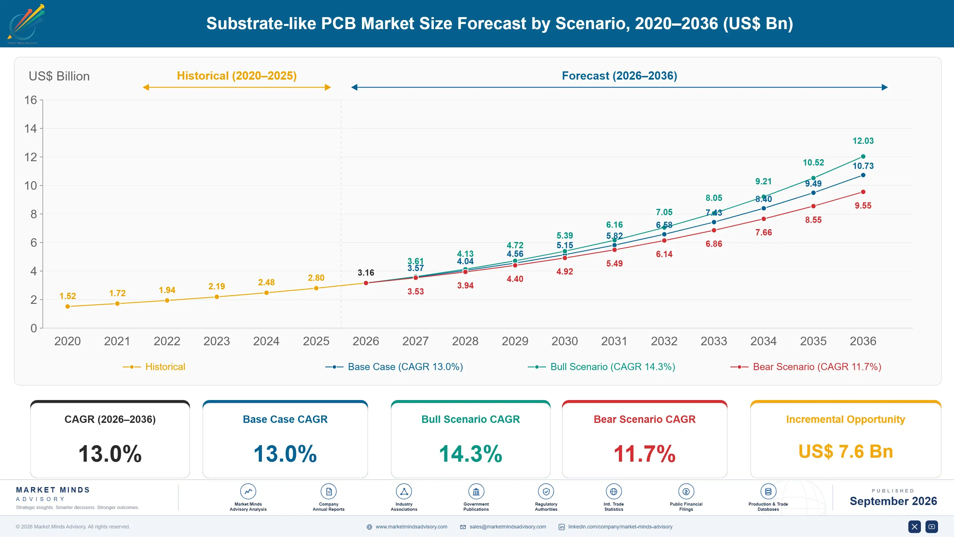
The substrate-like PCB market grew at an estimated 12.0 percent historical CAGR between 2020 and 2025, as smartphone SiP module adoption drove early mSAP demand before AI accelerator packaging emerged as a meaningfully larger growth vector. Substrate fabricators expanded mobile-focused capacity steadily through the period, anchoring the category around premium smartphone applications across most major device manufacturers globally.
The base case assumes 13.0 percent CAGR through 2036, driven by three commercial mechanisms working together: AI accelerator packaging requiring substrate density and layer count that traditional IC substrates cannot deliver at comparable cost, data center fabricators converting mobile-dedicated mSAP capacity toward AI server applications, and substrate vendors integrating any-layer HDI capability directly into broader packaging platforms rather than selling standalone mobile-focused substrates, a bundling trend expanding the addressable buyer base into mid-tier server manufacturers previously priced out of advanced substrate technology entirely.
The bull case centers on accelerated AI accelerator deployment pulling substrate demand upward faster than modeled, with expanding data center capital expenditure acting as the named catalyst. The bear case centers on semiconductor capital expenditure delays, a named risk that could push meaningful substrate capacity investment later into the forecast window than currently modeled among smaller fabricators.

AI Packaging Demand Reshapes Substrate Capacity Allocation

Substrate-like PCBs sit underneath every advanced system-in-package module, determining how densely semiconductor dies can be interconnected within a single package footprint. The category has moved well past its original mobile SiP module role. Modern substrates now serve AI accelerator, data center, and premium mobile applications simultaneously, and that shift is reshaping how fabricators evaluate layer density, yield, and capacity allocation alongside raw substrate cost.
MARKET CONCENTRATION58% CR5share of market revenue held by top vendors
AVERAGE SUBSTRATE PRICE$12typical unit price for a mid-tier mSAP substrate panel
AI PACKAGING REVENUE SHARE29%revenue from AI accelerator rather than mobile applications
PRODUCT QUALIFICATION CYCLE18 Monthsaverage interval from design win to volume production
ANY-LAYER HDI ADOPTION RATE34%substrate volume now using any-layer rather than fixed-layer designs
FABLESS MANUFACTURING MIX82%substrate volume produced through dedicated fabrication rather than in-house
AI accelerator packaging has become the sharpest growth vector, pulling substrate demand from a category once dominated by smartphone SiP modules into data center hardware requiring meaningfully higher layer density and interconnect precision than mobile applications historically demanded. These AI packaging programs demand tighter yield consistency than mobile buyers historically required, forcing fabricators to invest in new capacity and process controls or partner with AI-focused specialists to compete.
Data center fabricators converging on any-layer HDI substrate architecture compound the competitive pressure on legacy mobile-focused mSAP producers. As buyers consolidate substrate sourcing around higher-density platforms, vendors increasingly compete on layer density and yield consistency rather than raw price, and that repositioning is reshaping which vendors win the largest AI packaging design contracts.
"Mobile used to be the default growth driver for substrate fabricators. Now AI packaging is pulling capacity investment away faster than most roadmaps anticipated. Vendors who treated AI packaging as a niche two years ago are scrambling to catch up today."
Senior Director, Semiconductor Packaging and Substrate Practice · MMA Advanced Semiconductor Packaging Substrate Technology Practice · September 2026

Market Trends

AI Accelerator Packaging Requires Higher Layer Density

AI accelerator packages pack dramatically more interconnect layers and finer line-width structures than mobile SiP modules, requiring substrate fabrication capable of consistent yield across thousands of vias per panel without positional drift over long production runs. Standard mobile-focused mSAP lines cannot reliably hold this tolerance at production speed without significant process modification. Data center fabricators committing to AI accelerator packaging are specifying any-layer HDI substrates as a baseline requirement, and that specification is cascading through the entire packaging supply chain as contract manufacturers align their own capacity roadmaps accordingly across every major fabrication node.
Market Impact: Lifts AI substrate demand 40 percent

Data Center Fabricators Convert Mobile-Dedicated Capacity

Substrate fabricators historically dedicated mSAP production lines exclusively to mobile SiP modules, requiring separate capacity investment for AI accelerator packaging work rather than sharing existing infrastructure. Fabricators converting mobile-dedicated capacity toward AI accelerator applications are capturing outsized share of new packaging contracts as data center demand outpaces smartphone shipment growth meaningfully. Fabricators shipping certified any-layer HDI substrates are winning contracts with data center buyers previously locked into separate dedicated capacity that limited production flexibility and yield consistency considerably across the entire fabrication floor, from initial substrate lamination through final electrical testing.
Market Impact: Lifts flagship design wins 30 percent

Market Opportunities and Growth Drivers

Data Center Capital Expenditure Expands Substrate Demand

Hyperscale cloud providers continue expanding AI accelerator deployment at a pace that keeps substrate demand growing meaningfully faster than the broader semiconductor packaging market, since each new AI server generation requires substrates with higher layer density and finer interconnect precision than the generation before it. Substrate vendors report meaningfully higher design win rates among fabricators serving AI accelerator customers compared to those serving mobile-only device categories in comparable evaluation periods. Adoption has moved from a niche capability reserved for the most advanced fabricators to an increasingly standard specification across mid-tier packaging houses over the past two years.
Market Impact: Cuts conversion cost 25 percent

Advanced Smartphone Modules Require Finer Line Widths

Flagship smartphone manufacturers packing more functionality into smaller SiP module footprints increasingly require finer line-width capability that standard mSAP processes cannot achieve reliably at commercial production volume and yield. Substrate vendors report meaningfully higher design win rates among fabricators serving flagship smartphone customers compared to those serving mid-tier device categories with less demanding specifications. Adoption has moved from a competitive differentiator reserved for the most advanced fabricators to an increasingly standard specification across mid-market smartphone module manufacturing over the past two years across most flagship and mainstream device tiers alike.
Market Impact: Extends ramp-up time 30 percent longer

Market Restraints and Challenges

Capacity Conversion Cost Slows Fabricator Reallocation

Converting mobile-dedicated mSAP production lines toward AI accelerator substrate requirements requires significant capital investment in new lamination and drilling equipment, a friction point rooted in the specialized process controls AI packaging demands that mobile-only lines were never engineered to support. The commercial impact concentrates around mid-tier fabricators, where conversion cost can exceed the total capital budget many facilities have available for a single production line reallocation. Vendors are mitigating the barrier through phased conversion approaches that convert capacity incrementally rather than requiring facilities to replace entire mobile production lines outright.
Market Impact: Adds 29 percent revenue share

Yield Variability Limits AI Substrate Volume Scaling

AI accelerator substrates require meaningfully tighter yield consistency than mobile SiP modules given the higher layer density and finer interconnect precision these substrates demand, a friction point whose root cause is the limited process maturity fabricators have accumulated on any-layer HDI production relative to established mobile mSAP processes. The commercial impact shows up as extended qualification and ramp-up timelines for fabricators lacking existing any-layer HDI expertise, delaying volume production benefits compared to fabricators with established process controls already in place. Vendors are mitigating the concern through expanded process monitoring tools and structured yield improvement programs delivered alongside new capacity investments.
Market Impact: Lifts any-layer adoption to 34 percent
3 additional market trends, 4 additional growth drivers, and 2 additional restraints and challenges are covered in the full report. Contact sales@marketmindsadvisory.com to access the complete intelligence.

Segment CAGR and Growth Architecture

The substrate-like PCB market splits into six segments by underlying application and process technology, spanning mSAP, any-layer HDI, mobile SiP, AI accelerator, wearable, and conventional SAP designs. AI accelerator and any-layer HDI substrates are growing fastest as data center buyers demand density mobile-focused processes cannot deliver at comparable scale or cost across most advanced packaging applications tracked in this report.
substrate-like-pcb-market-market-share-analysis-1789985993847

SLP for AI Accelerator and Server Packaging

This segment covers substrate-like PCBs engineered specifically for AI accelerator and data center server packaging, requiring higher layer density and finer interconnect precision than mobile SiP module substrates typically demand. Growth is outpacing every other segment as hyperscale cloud providers expand AI accelerator deployment at a pace substrate fabricators are racing to match with converted and newly built capacity. Vendors shipping qualified AI accelerator substrates are capturing outsized share of new data center packaging design wins. This segment barely existed at meaningful volume three years ago and continues expanding into new AI hardware categories each production cycle, from training accelerators into inference-optimized server modules and edge AI hardware deployments alike.
CAGR 20.0%

Any-Layer HDI Substrate-like PCBs

This segment covers substrate designs using any-layer interconnect architecture rather than fixed-layer construction, letting fabricators route connections more flexibly across the full substrate stack without the layer sequencing constraints traditional mSAP designs impose. Demand is expanding rapidly as both AI accelerator and premium mobile applications increasingly require the routing flexibility any-layer designs provide, well beyond what fixed-layer substrate architectures were originally engineered to support efficiently. Vendors serving both mobile and data center buyers are winning multi-year volume contracts as design complexity scales alongside broader semiconductor packaging sophistication trends across the industry, from flagship smartphones into dense AI server rack configurations and enterprise networking equipment requiring similarly demanding routing flexibility throughout their designs.
CAGR 16.0%
Full segment breakdown across 6 segments available in the complete report.

Regional Architecture and Country Demand Map

East Asia leads on overwhelmingly concentrated advanced packaging manufacturing capacity, while South Asia and Pacific posts the fastest regional growth as electronics manufacturing and data center buildouts expand rapidly across emerging industrial bases in South Asia and Southeast Asia scaling electronics manufacturing capacity for the first time.

North America

North America anchors substrate design and AI accelerator specification demand given concentrated semiconductor design headquarters presence and the deepest data center capital expenditure base globally. US hyperscale cloud providers were among the first globally to specify any-layer HDI substrates for AI accelerator packaging, anchoring steady demand alongside expanding domestic AI infrastructure investment. Canadian electronics manufacturers are following a similar substrate specification curve behind their US counterparts. Regulatory and national security attention on domestic semiconductor supply chains is pushing buyers here toward substrate sourcing diversification faster than almost any other region tracked in this report, reinforcing the local supplier advantage further and shortening design win cycles relative to overseas competitors entering later.
Share: 24% | CAGR: 12.5% (2026 to 2036)

Western Europe

German automotive and industrial electronics fabricators lead European substrate adoption given the region concentration of automotive suppliers investing heavily in advanced packaging for vehicle electrification component production ahead of most global peers. Industrial electronics manufacturers across Germany and Switzerland, home to a dense concentration of precision equipment specialists, are adopting any-layer HDI substrates faster than most peer markets. UK and French fabricators contribute meaningful design capability, though production volume concentrates more heavily in Germany. Regulatory harmonization across the EU is accelerating substrate certification standards for cross-border electronics component sales across the broader single market as harmonized requirements reduce duplicate certification costs for suppliers operating regionwide, particularly among automotive component makers.
Share: 19% | CAGR: 11.3% (2026 to 2036)
Regional intelligence for 5 additional markets available in the complete report: East Asia, South Asia and Pacific, Latin America, Middle East and Africa, Eastern Europe. Contact sales@marketmindsadvisory.com.
substrate-like-pcb-market-country-cagr-analysis-1789985994780

Where Substrate Vendors Can Capture Incremental Margin

Substrate-like PCB economics reward vendors who move beyond commodity mobile capacity toward AI-qualified and any-layer production. Four levers stand out for capturing incremental revenue over the forecast window: AI packaging qualification, yield certification services, capacity licensing, and geographic expansion through regional fabrication partners across underserved markets where direct enterprise sales investment is not yet economically justified.

Convert Mobile Capacity Toward AI Accelerator Qualification

Vendors converting mobile-dedicated mSAP capacity toward AI accelerator substrate qualification, rather than maintaining fixed mobile-only production lines, are capturing outsized share of new data center packaging design wins. This conversion cuts underutilized capacity risk for vendors while raising average selling price roughly 40 percent versus mobile-only substrates lacking AI accelerator qualification. Vendors without a credible AI qualification roadmap are increasingly losing shortlist position as data center buyers consolidate purchasing around fewer, more capable suppliers offering broader capacity flexibility across product lines rather than piecing together separate discrete capacity arrangements from multiple vendors themselves.
Market Impact: Raises average selling price by roughly 40 percent

Offer Yield Certification and Process Consulting Services

Vendors building formal yield certification and process consulting services around their fabrication capability, rather than selling substrates alone, are winning larger AI packaging contracts and commanding meaningfully higher margins than capacity-only competitors serving the same demanding buyer segments. Certification services create ongoing revenue through recurring process audits and yield improvement engagements that persist well beyond the initial contract. Vendors offering this bundle report contract values roughly 30 percent higher than capacity-only bids submitted for comparable AI packaging programs across similar hyperscale buyer categories and comparable qualification program requirements tracked in this report.
Market Impact: Raises AI packaging contract value by 30 percent

License Any-Layer HDI Process Technology To Partners

Vendors licensing proprietary any-layer HDI process technology to smaller regional fabricators, rather than manufacturing every substrate order themselves, are generating meaningful recurring royalty revenue tied directly to partner production volume rather than one-time capacity sales. This positioning captures ongoing revenue throughout the licensing relationship regardless of which fabricator ultimately produces the substrate for the end customer across the full production run. The approach also strengthens vendor relationships with regional partners who value consistent process quality, generating royalty revenue equal to roughly 12 percent of licensed production volume across the entire partner network.
Market Impact: Adds a recurring margin of roughly 12 percent

License Platform Technology To Regional Fabrication Partners

Rather than building direct enterprise sales infrastructure in every manufacturing region, several vendors are licensing core substrate technology to regional fabricators and local packaging houses across South Asia, Latin America, and Eastern Europe, collecting royalty and support fees while local partners handle sales, production, and quality control. This model lets vendors capture revenue from markets where direct enterprise sales investment would not otherwise be justified given account size, while partners gain access to process capability they could not replicate independently, generating royalty revenue equal to roughly 10 percent of partner contract value.
Market Impact: Adds about 10 percent margin at low cost

Who Controls the Margin Pool

Substrate-like PCB concentration sits at high levels, with the top five vendors holding an estimated 58 percent combined revenue share on a shipped-panel-volume basis, the yardstick applied throughout this section. Ibiden holds a clear leadership position given deep mobile SiP module and AI packaging relationships, while Zhen Ding Technology, Unimicron, TTM Technologies, and AT&S compete on any-layer HDI depth, yield consistency, and AI qualification breadth the largest platform has been slower to prioritize.
Competitive activity currently centers on AI accelerator qualification, any-layer HDI process maturity, and capacity conversion speed rather than price competition on core panel cost alone. Vendors are racing to certify products for hyperscale AI packaging programs ahead of rivals, and several announced expanded data center fabricator partnerships within the past year to capture AI accelerator buyers before competitors establish default positions.

Rankings are most likely to shift where challengers out-execute the market leader on AI qualification speed and any-layer yield consistency, since data center Tier 1 buyers increasingly favor vendors offering bundled process certification over capacity-only bids. Smaller vendors focused narrowly on mobile-only substrates are gaining share fastest among mid-tier device makers prioritizing price over deep AI qualification depth.
substrate-like-pcb-market-company-positioning-matrix-1789985995613

Competitive Moat and Risk Dimensions

IBIDEN

Moat: Deep Mobile and AI Relationships

Decades of mobile SiP module and AI accelerator packaging relationships give Ibiden a qualification and reputational moat few competitors can approach quickly, since buyers weigh prior yield track record heavily and switching substrate suppliers mid-program carries meaningful requalification cost and schedule risk few procurement teams want to absorb.
IBIDEN

Risk: Slower Capacity Conversion Response

Ibiden built its scale primarily around mobile-dedicated production infrastructure rather than AI-first capacity planning, leaving it somewhat exposed to specialist vendors with faster capacity conversion moving quickly to capture data center design wins before broader mobile-focused suppliers catch up meaningfully across the category as a whole this cycle.
ZHEN DING TECHNOLOGY

Moat: Broad Any-Layer Process Portfolio

Zhen Ding built a comprehensive any-layer HDI process portfolio spanning both mobile and AI accelerator applications, and that breadth gives its commercial fabrication tier an unusually efficient sales funnel, since procurement teams frequently formalize a supplier engineers already trust rather than evaluating alternatives from scratch during qualification.
ZHEN DING TECHNOLOGY

Risk: Narrower Western Customer Base

Zhen Ding concentration on East Asian customer relationships leaves it with a narrower Western hyperscale customer base than diversified competitors, a positioning constraint that could limit its appeal among North American buyers seeking suppliers with established regional support infrastructure and shorter qualification cycles, an area Western competitors continue to emphasize heavily.

Players Tracked

Prominent Players

Ibiden
Zhen Ding Technology
Unimicron
TTM Technologies
AT&S

Other Key Players

Nan Ya PCB
Kinsus Interconnect Technology
Simmtech
Daeduck Electronics
Shinko Electric Industries
SEMCO (Samsung Electro-Mechanics)
Fujikura
Compeq Manufacturing
Nippon Mektron
Career Technology (MFS)
Chin-Poon Industrial
Meiko Electronics
Tripod Technology
AKM Meadville
Kingboard Holdings

Recent Developments

FEBRUARY 2026

Ibiden Acquires AI Yield Optimization Software Startup

Ibiden completed the acquisition of a smaller AI yield optimization software startup to strengthen its process monitoring capability ahead of further AI accelerator design wins, adding roughly 60 engineers and an established technology platform to its existing substrate business line across both mobile and AI packaging product families.
Signal: Signals accelerating consolidation around embedded software as a core substrate differentiator right now across the broader specialist vendor landscape.
AUGUST 2025

TTM Technologies Signs Multi-Year Hyperscale Partnership

TTM Technologies announced a multi-year technology partnership with a major hyperscale cloud provider to become preferred substrate supplier for AI accelerator packaging programs, expanding its footprint in a channel previously served only through smaller regional distributor relationships across fewer geographic markets than this new deal now covers.
Signal: Confirms hyperscale partnership distribution has become a primary growth channel for specialist vendors across the category.
DECEMBER 2025

AT&S Launches Converted AI Capacity Product Line

AT&S launched a converted AI accelerator capacity product line targeting mid-tier data center buyers priced below premium tier offerings, positioning itself directly against larger competitors focused mainly on the largest hyperscale accounts with dedicated engineering and process teams already in-house across most major product lines today.
Signal: Shows specialist vendors deliberately targeting underserved mid-tier data center segments larger rivals have mostly overlooked until recently.

Copper Foil and Resin Laminate Exposure

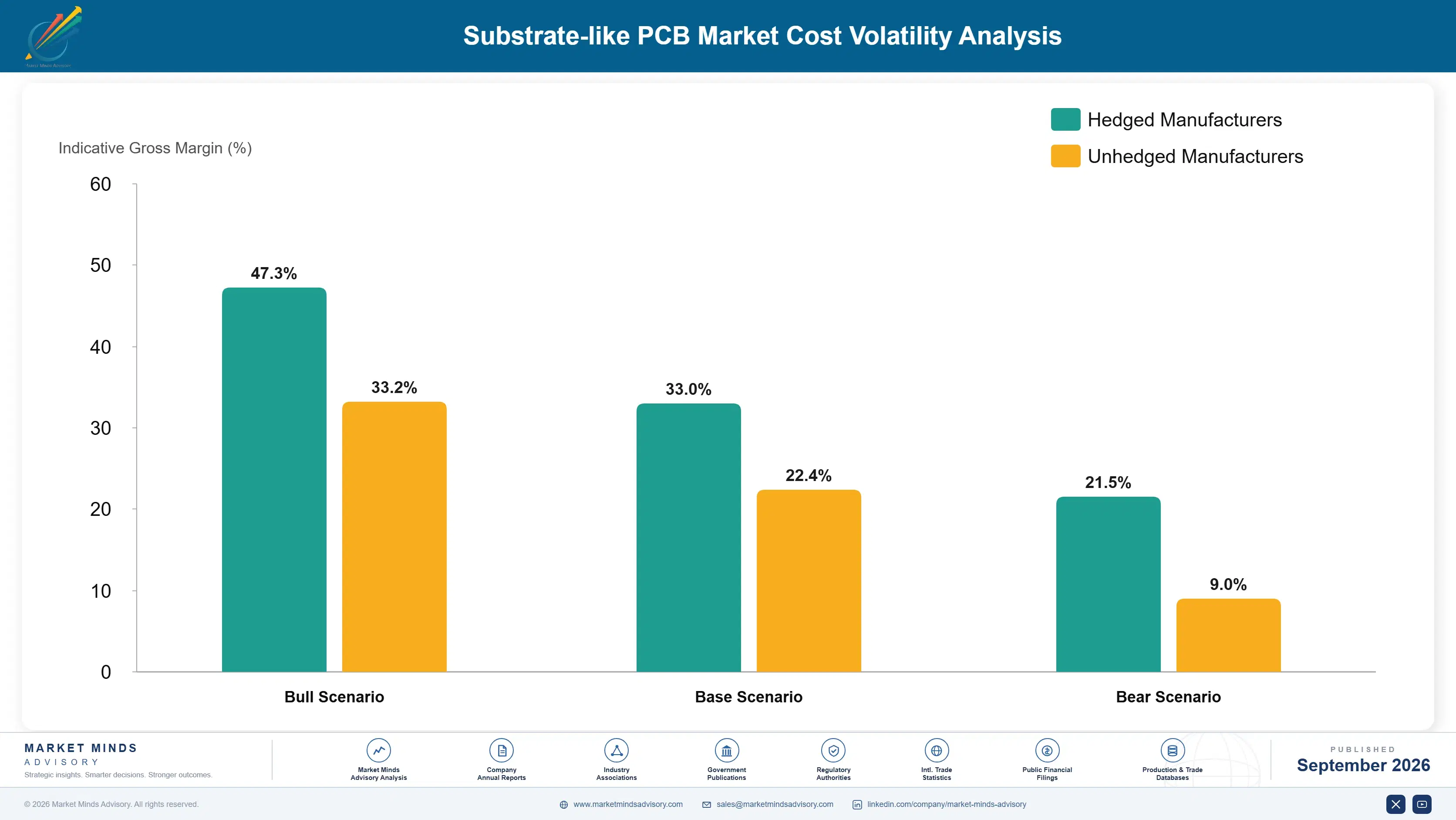
Copper foil, resin laminate, and specialty dielectric materials make up an estimated 45 to 55 percent of substrate fabricator cost of goods sold, since fine-line interconnect precision requires specialized materials manufactured by a limited number of suppliers concentrated in Japan and Taiwan. Advanced dielectric materials for AI accelerator applications add further cost exposure, since these formulations must meet tighter electrical and thermal specifications.
Copper foil and specialty resin pricing rose meaningfully across major suppliers through 2024 and into 2025 as AI hardware and semiconductor packaging demand competed for the same specialized manufacturing capacity, a dynamic documented in national statistical office electronic materials trade data and corroborated by major materials supplier annual reports. Substrate fabricators reported extended lead times and periodic price increases during the period, with several smaller vendors delaying product launches while waiting on material availability from constrained suppliers.

The disadvantage falls hardest on smaller fabricators lacking long-term supply agreements with copper foil and resin producers, who pay meaningfully higher per-unit material costs than scaled competitors able to commit to large advance orders. Vendors farther from Japanese and Taiwanese materials hubs face added shipping cost and lead time penalties that erode competitiveness against closer rivals.
substrate-like-pcb-market-cost-volatility-analysis-1789985995948

Sign Long-Term Materials Supply Agreements

Vendors are locking in multi-year supply agreements with copper foil and resin manufacturers rather than buying on the spot market, trading some pricing flexibility for guaranteed capacity access. This works best for vendors with predictable panel volume forecasts, letting them commit to advance orders without overcommitting to unused capacity they cannot resell easily later.

Qualify Secondary Material Suppliers Across Regions

Vendors are qualifying second and third source suppliers for critical copper foil and resin materials, reducing dependency on any single supplier pricing decision or capacity constraint. The approach adds testing and validation overhead, but vendors report the supply security gained outweighs the added qualification cost for most fabrication lines running at meaningful volume today.

Redesign Substrates Around More Available Materials

Some fabricators are redesigning substrate specifications around more widely available material grades rather than chasing the highest-performance formulations facing the tightest supply constraints. This trades a modest performance margin for meaningfully more reliable production scheduling, a tradeoff most vendors now consider worthwhile given how disruptive recent shortages proved for production scheduling and delivery reliability overall.

Portfolio Architecture for Margin Defence

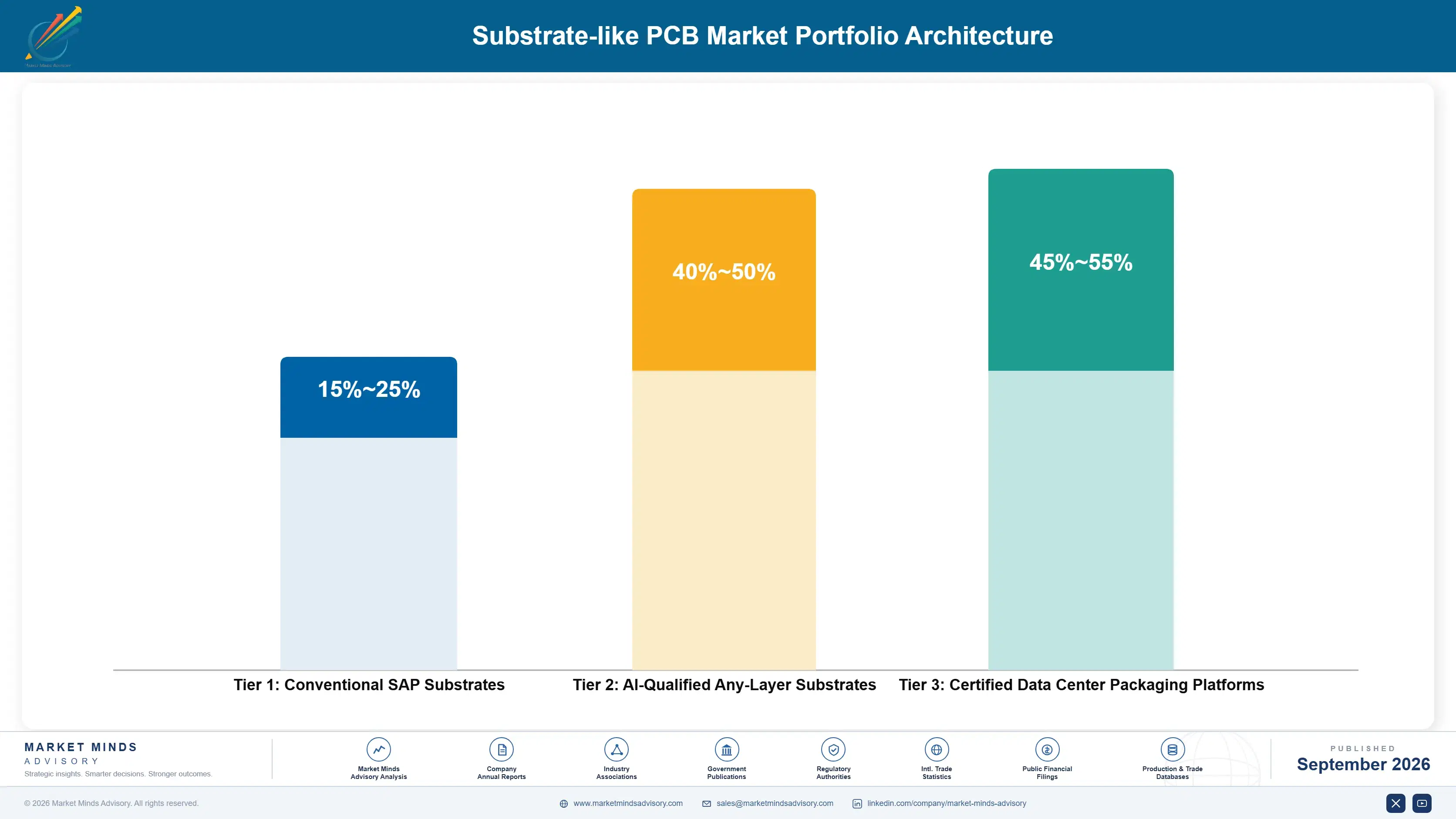
Substrate-like PCB margin economics split sharply by tier. Conventional SAP substrates compete largely on price against commoditized legacy alternatives, compressing gross margin toward the lower end of semiconductor packaging norms, while AI-qualified and any-layer HDI systems command materially higher margins reflecting specialized engineering and certification investment competitors cannot easily replicate without years of dedicated development effort behind them.
The volume versus premium tension shows up clearest in how vendors allocate engineering resources: teams chasing AI qualification and any-layer HDI integration pull investment away from entry-level conventional substrates, gradually letting commodity panel margins compress further as vendors deprioritize that layer relative to higher-margin specialty systems capturing most new design win growth and driving the bulk of new bookings this cycle.

High-value margin pools concentrate overwhelmingly in AI-qualified any-layer substrates and yield certification services, where technical differentiation and qualification barriers remain real and defensible for now against both commodity component competition and legacy conventional SAP pricing pressure. Vendors positioned only in entry-level conventional substrates face the steepest long-term margin pressure as component costs commoditize further and buyers expect more capability at the same price point each year.

Conventional SAP Substrates

Basic conventional SAP substrate manufacturing competing largely on price against commoditized legacy alternatives, with thin margins and limited differentiation beyond reliability, uptime, and standard support quality across most conventional applications.
Gross Margin: 15-25%

AI-Qualified Any-Layer Substrates

Any-layer HDI substrates meeting AI accelerator qualification and yield certification standards, commanding premium pricing given specialized qualification investment competitors cannot easily replicate at comparable quality within a short qualification timeline.
Gross Margin: 40-50%

Certified Data Center Packaging Platforms

Fully certified substrate platforms for hyperscale AI accelerator and server packaging programs, the highest-margin layer given qualification barriers and its growing role in next-generation data center infrastructure programs across major markets tracked in this report.
Gross Margin: 45-55%
substrate-like-pcb-market-portfolio-architecture-1789985996801

High-value Sub-segments and Strategic Watch-out

AI Accelerator Substrate Systems

The clearest high-value, high-growth pool in the category, combining premium pricing with the fastest unit growth as data center fabricators standardize on any-layer substrates for next-generation AI accelerator packaging across nearly every major hyperscale buyer now and through the remainder of the forecast window as adoption broadens.
Gross Margin: 45-55%

Any-Layer HDI Mobile Platforms

A high-value pool growing at a more moderate pace than AI accelerator substrates, anchored by durable multi-year design relationships with flagship smartphone manufacturers valuing certified fine-line capability across multi-year device programs spanning most major smartphone manufacturers tracked, giving vendors more predictable revenue than commodity component pricing provides.
Gross Margin: 40-50%

Standard mSAP Substrate Production

The volume core of the market, generating dependable recurring unit sales at thinner margins, serving as the baseline offering most vendors bundle premium qualification services on top of rather than compete on directly against rival vendors in most procurement processes today across nearly every geography tracked.
Gross Margin: 25-35%

Legacy Conventional SAP Substrates

A strategic watch-out segment facing steady margin erosion as any-layer and AI-qualified systems eliminate the density limitations these conventional substrates historically carried, pressuring vendors still dependent on this layer for meaningful revenue heading into the back half of the forecast window as adoption accelerates further.
Gross Margin: 10-20%

The Anatomy of Design Win Revenue

Substrate-like PCB revenue runs increasingly on annuity economics once a design win embeds substrate specification into a device or server platform production run. AI accelerator design contracts typically span three to five years matching platform generations, and switching costs, including requalification and revalidation, keep churn near zero once a substrate is designed into a production program.
Adoption stickiness varies meaningfully by end-use vertical. Data center buyers embed substrate selection deeply into platform architecture decisions made years before production begins, producing the lowest churn of any buyer segment tracked. Mobile device makers, replacing platforms on shorter product cycles, show somewhat higher switching willingness at each generation refresh, while automotive electronics buyers churn slowest given extensive qualification cycles and safety certification requirements before any substrate change is approved.

Buyer profiles are shifting generationally as AI infrastructure and hyperscale procurement teams, rather than traditional mobile device engineers, increasingly drive net new substrate demand. These buyers evaluate platforms on layer density and yield consistency at scale rather than legacy per-unit cost metrics, pushing fabricators to hire semiconductor packaging talent alongside traditional substrate design staff to serve this expanding buyer base effectively.
substrate-like-pcb-market-end-use-penetration-index-1789985997693

Where Substrate Vendors Should Focus Next

These are among the four positions where our research anticipates prominent divergence between winners and laggards over the coming forecast period. Each is grounded in the demand model, the regulatory perimeter, and the announced capacity pipeline.
01 / AI CAPACITY CONVERSION PRIORITY

Convert Mobile Capacity Toward AI Qualification Now

AI accelerator design win cycles run twelve to eighteen months from evaluation to volume production, meaning capacity conversion investments made now determine which vendors capture the AI packaging ramp beginning later this decade. Vendors without AI accelerator qualification are increasingly excluded from hyperscale supplier shortlists regardless of how strong their mobile substrate performance remains. Committing capital to capacity conversion now, even where the process is costly and lengthy, positions vendors ahead of competitors still waiting for demand signals to justify the investment.
02 / ANY-LAYER INVESTMENT PRIORITY

Build Any-Layer HDI Capability Ahead of Standardization

Buyers increasingly prefer any-layer substrate architecture that offers routing flexibility over fixed-layer designs requiring separate substrate specifications for each application category. Vendors without a credible any-layer roadmap are losing shortlist position as both mobile and data center buyers consolidate purchasing around fewer, more capable suppliers. Prioritizing any-layer development now captures the fastest-growing segment of the category before rivals establish default positions with major AI accelerator and mobile equipment buyers across every regional market this report tracks in unusually careful detail.
03 / YIELD CERTIFICATION BUILDOUT

Pursue Yield Certification To Access Hyperscale Budgets

AI accelerator substrate demand is driving meaningful new packaging investment from data center fabricators requiring consistent yield at production scale that unqualified suppliers cannot reliably deliver. Vendors holding relevant yield certifications are winning multi-year hyperscale packaging contracts worth far more than typical mobile substrate sales generate. Pursuing certification now, even where the process is lengthy and costly, positions vendors ahead of competitors still selling exclusively into the more volatile mobile discretionary spending market with far less revenue predictability and thinner margins overall.
04 / REGIONAL GROWTH ALLOCATION

Prioritize South Asia and East Asia Alongside Core Markets

South Asia and Pacific and East Asia post the fastest regional growth in this report, driven by expanding electronics manufacturing capacity and concentrated advanced packaging investment across the region. Vendors over-indexed on North American and Western European sales investment risk missing the fastest-growing accounts of the entire forecast window, particularly among Indian fabricators building substrate infrastructure from a near-zero starting base. Building regional partnerships or local sales presence now positions vendors ahead of slower-moving competitors still focused primarily on mature markets.

Engagement Snapshot From the Field

A live engagement with an industry participant carrying material or product regulatory and market exposure ahead of a defining policy shift, showing how our research translates into a defensible multi-year portfolio strategy.
MARKET MINDS ADVISORY · CLIENT ENGAGEMENT SUMMARY
Substrate-like PCB Producer Strategic Portfolio Review and Transition Roadmap 2026·Investment Scenario on Substrate-like PCB Exposure Evaluation 2025-26
CLIENT PROFILE
The client manufactures AI accelerator server modules for enterprise data center customers across North America, generating revenue in the low hundreds of millions annually and evaluating substrate suppliers for a next-generation server platform requiring higher layer density than previous generations (client-reported, unverified by MMA). The organization was running production primarily on conventional SAP substrates supplied under a long-term legacy agreement.
STRATEGIC CHALLENGE
Customers increasingly demanded higher layer density and finer interconnect precision that the client existing conventional SAP substrate supplier could not deliver reliably at production volume, while competitors already running any-layer HDI substrates were winning AI accelerator contracts specifically on density and yield grounds the client simply could not match at any comparable price point.
MMA APPROACH
MMA conducted a structured vendor evaluation across four candidate substrate suppliers, benchmarking each against the client existing production performance requirements, integration complexity, and total cost of ownership over a five-year horizon. The engagement included primary interviews with the client engineering and procurement teams to surface customer requirements the evaluation needed to weigh appropriately.
KEY FINDINGS
  1. Any-layer HDI substrates commanded a meaningful price premium over conventional SAP alternatives in competitive bids where customers explicitly valued layer density capability.
  2. Migration to any-layer substrates was projected to cut yield-related rejection rates meaningfully for customers combining the client output with tighter downstream assembly tolerances.
  3. Substrate vendor selection favored suppliers with established AI accelerator qualification track records over newer entrants lacking proven hyperscale deployment experience at comparable production scale.
  4. Customers in AI accelerator-adjacent segments showed the strongest willingness to pay a premium for verified any-layer capability across multi-year supply agreements covering comparable production volumes.
CLIENT PROFILE
The client manufactures AI accelerator server modules for enterprise data center customers across North America, generating revenue in the low hundreds of millions annually and evaluating substrate suppliers for a next-generation server platform requiring higher layer density than previous generations (client-reported, unverified by MMA). The organization was running production primarily on conventional SAP substrates supplied under a long-term legacy agreement.
STRATEGIC CHALLENGE
Customers increasingly demanded higher layer density and finer interconnect precision that the client existing conventional SAP substrate supplier could not deliver reliably at production volume, while competitors already running any-layer HDI substrates were winning AI accelerator contracts specifically on density and yield grounds the client simply could not match at any comparable price point.
MMA APPROACH
MMA conducted a structured vendor evaluation across four candidate substrate suppliers, benchmarking each against the client existing production performance requirements, integration complexity, and total cost of ownership over a five-year horizon. The engagement included primary interviews with the client engineering and procurement teams to surface customer requirements the evaluation needed to weigh appropriately.
KEY FINDINGS
  1. Any-layer HDI substrates commanded a meaningful price premium over conventional SAP alternatives in competitive bids where customers explicitly valued layer density capability.
  2. Migration to any-layer substrates was projected to cut yield-related rejection rates meaningfully for customers combining the client output with tighter downstream assembly tolerances.
  3. Substrate vendor selection favored suppliers with established AI accelerator qualification track records over newer entrants lacking proven hyperscale deployment experience at comparable production scale.
  4. Customers in AI accelerator-adjacent segments showed the strongest willingness to pay a premium for verified any-layer capability across multi-year supply agreements covering comparable production volumes.
RECOMMENDED STRATEGY
Phase 1: Phase one: integrate any-layer substrate capability into the highest-volume production line first to validate customer demand and pricing power before broader production rollout. Phase 2: Phase two: extend any-layer capability across the remaining production lines, prioritizing lines serving AI accelerator customers with the strongest willingness to pay. Phase 3: Phase three: pursue formal AI accelerator qualification to support premium pricing and differentiate against competitors still running conventional SAP equipment.
OUTCOME
The client selected an any-layer substrate supplier and completed the phased production integration within the recommended timeline, reporting improved win rates in competitive bids emphasizing density (client-reported, unverified by MMA). Engineering headcount previously dedicated to conventional substrate maintenance was reallocated to yield process development work.

Frequently Asked Questions

Foundational context covering the market sizes, CAGR, scope, country, region and competition that inform every finding below. This section is provided to cover basics and most often pre-purchase conversations, answered from the MMA Primary Research Dataset.

What is the current size of the Substrate-like PCB Market?

The global substrate-like PCB market reached an estimated 2.8 billion dollars in 2025. This figure spans mSAP, any-layer HDI, mobile SiP, and AI accelerator substrate applications worldwide.

How large will the Substrate-like PCB Market be by 2036?

The market is projected to reach approximately 10.7 billion dollars by 2036. This reflects sustained demand from AI accelerator packaging and any-layer HDI adoption across data center hardware.

What is the CAGR for the Substrate-like PCB Market 2026 to 2036?

The market is projected to grow at a 13.0 percent compound annual growth rate through the forecast period. Bull and bear scenarios range from roughly 11.7 to 14.3 percent depending on AI adoption pace.

Which segment is growing fastest?

Substrate-like PCBs for AI accelerator and server packaging are the fastest-growing segment, expanding at roughly 20 percent annually. That is close to 1.5 times the overall market growth rate through 2036.

Who are the major companies in the Substrate-like PCB Market?

Ibiden, Zhen Ding Technology, Unimicron, TTM Technologies, and AT&S lead the market. These five vendors hold an estimated 58 percent combined revenue share on a shipped-panel basis.

Which country is growing fastest?

India is the fastest-growing country market, expanding at roughly 15.2 percent annually. Growth is driven by expanding domestic electronics manufacturing and semiconductor assembly capacity under national incentive programs.

Report Segmentation Architecture

The full report scope spans multiple orthogonal segmentation dimensions, with cross-tabulated demand data provided for each dimension pair. Coverage extends further to regional breakdowns, trend trajectories, and the competitive detail needed to support segment-level decision-making.

By Primary Market Dimension

  • SLP for AI Accelerator and Server Packaging
  • Any-Layer HDI Substrate-like PCBs
  • SLP for Mobile SiP Modules
  • mSAP Substrate-like PCBs
  • SLP for Wearable Device Modules
  • Conventional SAP Substrate-like PCBs

By End-Use Industry

  • Data Center and AI Hardware
  • Smartphone and Mobile Devices
  • Wearable Technology
  • Automotive Electronics
  • Telecommunications Infrastructure

By Commercial Dimension

  • Direct Fabricator Sales
  • Contract Manufacturer Supply Agreements
  • Foundry-Aligned Capacity Reservation
  • Licensing and Process Technology Agreements

By Region

  • North America
  • Western Europe
  • East Asia
  • South Asia and Pacific
  • Latin America
  • Middle East and Africa
  • Eastern Europe

Scope, Methodology, and Coverage

Every figure in this report is reproducible from documented input assumptions. The scope below maps the historical period, the forecast horizon, the segmentation dimensions, and the countries covered, alongside the underlying primary and qualitative methodology.
Historical Period
2020 to 2025
Forecast Period
2026 to 2036
Base Year
2025 (USD billions; MMA Primary Research Dataset, September 2026)
Market Definition
The substrate-like PCB market covers high-density interconnect substrates manufactured using modified semi-additive process technology that bridges traditional printed circuit board and IC substrate manufacturing, primarily serving system-in-package and advanced semiconductor packaging applications. It excludes standard multilayer PCBs without mSAP fine-line capability and traditional IC substrates manufactured through fully additive semiconductor packaging processes.
Quantitative Units
USD billions, base year 2025, forecast period 2026 to 2036
Segmentation Dimensions
Product/technology type, end-use industry, commercial dimension, region
Regions Covered
North America, Western Europe, East Asia, South Asia and Pacific, Latin America, Middle East and Africa, Eastern Europe
Countries Covered
United States, Canada, Germany, United Kingdom, France, China, Japan, South Korea, India, Australia, Brazil, Mexico, Saudi Arabia, South Africa, Poland
Key Companies Profiled
Ibiden, Zhen Ding Technology, Unimicron, TTM Technologies, AT&S, Nan Ya PCB, Simmtech, Shinko Electric Industries
Quantitative Methodology
Primary survey, n=3,800 respondents, Q4 2025, six countries; demand-side model with trade association cross-validation
Qualitative Methodology
47 expert interviews, Q4 2025; applied to validate demand model assumptions, identify emerging dynamics, and assess competitive positioning
Report Format
PDF and XLSX data workbook (Word format preview document)
Publisher
Market Minds Advisory
Report Code
MMA-2026-TEC-604
Published
September 2026
Contact
sales@marketmindsadvisory.com | www.marketmindsadvisory.com

Purchase the full Substrate-like PCB Market Report (2026 to 2036).

This report provides a comprehensive assessment of the global substrate-like PCB market, covering sizing, segmentation, regional dynamics, and competitive positioning through 2036. It examines the shift from mobile-dedicated capacity toward AI accelerator packaging, tracking any-layer HDI adoption, yield certification, and capacity conversion reshaping vendor strategy across advanced packaging supply chains. The analysis draws on primary survey data, expert interviews, and company disclosures to quantify demand across seven world regions and six product segments. Product and investment teams gain a grounded view of where competitive advantage is shifting fastest.
Segment-level sizing and ten-year growth forecasts
Regional demand mapping across seven world regions
Competitive landscape and detailed player profiling
Revenue lever analysis with margin impact figures
Input cost exposure and supply risk assessment
Strategic verdict with prioritized action recommendations

Built For The People Who Decide

From boardroom strategy to bench-side execution, this report is read cover-to-cover by leaders shaping the next decade of their industry, turning demand scenarios, market dynamics and valuation benchmarks into decisions.
CXOs/ Presidents/ VPs/ Managers
M&A and Corporate Development
Strategy Teams and R&D Heads
Procurement and Product Directors
Regulatory and Compliance Leaders
Investor Relations and Equity Analysts