

Market Minds Advisory
Photonic Integrated Circuit Market

Photonic Integrated Circuit Market: Photonic Integrated Circuit Market: Packaging Cost, Platform Choice and Foundry Access 2026 to 2036

The chip is the cheap part. Getting light into it and back out again costs more than fabricating it did, and that single ratio has governed this industry for twenty years.

Lead Analyst

Published

September 2026

Make Smarter Decisions with Customized Research Insights

Request a free sample report and evaluate market opportunities, growth trends, and competitive dynamics relevant to your business needs.

2025 MARKET VALUE$8.9BMarket Size 2025
2036 FORECAST VALUE$36.5BBase Case , 2026 to 2036
CAGR 2026 TO 203613.6 %Bull 14.9% / Bear 12.3%
INCREMENTAL OPPORTUNITY$26.3BNet 10- year value creation
EXPANSION MULTIPLE3.58x2036 value over 2026 base
Strategic Levers
M&A Pipeline
Regional Outlook
Country Rankings
Competitive Intelligence
Segmental Deep-dive
Call-Us : 91 93563 13602

Executive Snapshot and Market Trajectory.

The photonic chip is the cheap part of a photonic product. Getting light into it and back out again costs a good deal more than fabricating it did, and that single ratio has governed this industry for two decades without moving very much at all.
The market reaches USD 10.2 billion in 2026 and USD 36.5 billion by 2036, a 3.58 times expansion at 13.6% annually. Silicon photonics for optical interconnect grows at 20.4%, half again the market rate of 13.6%, because data centre link demand keeps rising faster than copper can carry it at distance. East Asia holds 35% of global value, above the usual band ceiling, on the assembly and packaging capacity concentrated across the region.
Five suppliers hold 52% of all photonic chip and module revenue worldwide, and vertical integration explains considerably more of that concentration than any difference in fabrication capability does. Broadcom, Coherent, Lumentum, Intel and Cisco Systems lead the field between them. A firm holding both chip design and its own packaging capacity controls the single cost line that decides whether a photonic product is commercially viable at all.
Market Definition
This report covers photonic integrated circuits and the modules built from them, by material platform: silicon photonics for optical interconnect, indium phosphide active photonic circuits, silicon nitride passive and low-loss circuits, lithium niobate high-speed modulator circuits, gallium arsenide photonic devices, and hybrid and heterogeneously integrated assemblies. It excludes discrete lasers and detectors not integrated onto a photonic circuit, optical fibre and cable, passive optical components, test equipment, and complete network systems or transceivers sold without integrated photonics.
Base Year Value
$8.9B in 2025 (MMA Primary Research Dataset, September 2026)
Forecast Period
2026 to 2036, eleven discrete annual values
CAGR
13.6% base case. Bull 14.9%. Bear 12.3%.
Fastest Growth Segment
Silicon Photonics For Optical Interconnect: 20.4% CAGR
Fastest Growth Country
India: 21.7% CAGR
Fastest Growth Region
South Asia and Pacific: 15.8% CAGR
Largest Region
East Asia: 35% of 2025 global value
Market Leaders
Broadcom, Coherent, Lumentum, Intel and Cisco Systems lead on photonic integrated circuit and module revenue. Source: MMA Analysis.
Primary Survey
n=3,800 procurement and R&D decision-makers, Q4 2025, six countries
Methodology
Demand-side build-up, cross-validated against public data, 47 expert interviews

Photonic Integrated Circuit Market Forecast Scenarios

photonic-integrated-circuit-market-size-forecast-scenario-1789994976565
Between 2020 and 2025 the category compounded at 12.4%, and the demand came from somewhere most of the industry had not been designing for. Data centre interconnect requirements rose faster than copper links could serve, which pulled silicon photonics into volume production. Telecom transport, the traditional application, grew far more slowly. Packaging capacity became the delivery constraint well before wafer capacity did.
The base case holds 13.6% on three mechanisms. Data centre link demand keeps rising with distributed computing workloads, and copper runs out of reach at the distances and rates now required. Co-packaged optics moves photonics onto the switch package itself, which raises photonic content per system substantially. And sensing applications across automotive, medical and industrial instrumentation keep adopting integrated photonics in places where discrete optical assemblies were previously used instead.
The bull case at 14.9% assumes co-packaged optics reaches volume deployment on the announced timetable, which would multiply photonic content across every switch shipped. The bear case at 12.3% is packaging capacity: if assembly and test capacity does not expand alongside wafer supply, delivery constraints cap the market well below what design activity and customer demand would otherwise support.

Packaging Costs More Than Fabrication

One number explains the shape of this industry. Assembly, alignment and test account for roughly 64% of what a finished photonic device costs, which means the wafer is the smaller half of the problem. Getting a fibre positioned to within half a micron of a waveguide, holding it there through thermal cycling and testing that the light actually goes where it should is expensive work that has resisted automation far longer than anybody expected.
TOP FIVE CONCENTRATION52%Held by vertically integrated firms rather than pure chip designers
PACKAGING COST SHARE64%Assembly, alignment and test within total delivered device cost
FIBRE ALIGNMENT TOLERANCE0.5 micronsPositioning accuracy required for acceptable optical coupling efficiency
FOUNDRY TAPE-OUT CYCLE11 monthsFrom design submission to returned wafers for evaluation
COUPLING LOSS BUDGET1.5 decibelsTypical penalty getting light onto and off the circuit
DESIGN REUSE RATE23%Circuit blocks carried directly between successive product generations
That cost structure is why vertical integration matters more here than in electronic semiconductors. A firm that designs the chip but buys packaging is subcontracting the majority of its cost to somebody else, with limited ability to improve it. The five leading suppliers are integrated across design, fabrication and packaging, and that is a better explanation of their position than any argument about who has the best circuit designs.
Demand has also shifted underneath the industry. Telecom transport drove photonics for years and grew modestly; data centre interconnect arrived and grew far faster, pulling silicon photonics into genuine volume at 20.4% against 13.6% for the market. Suppliers built around telecom qualification cycles found themselves selling to a customer reordering quarterly and expecting cost reduction every generation.
"Every few years somebody announces a photonic circuit with remarkable performance and then cannot ship it, because putting a fibre on it costs three times what the chip did. Fabrication stopped being the hard part a long time ago. Almost nobody's investment case reflects that yet."
Director, Photonics and Optical Semiconductor Practice · MMA Technology Practice · September 2026

Market Trends

Data Centre Interconnect Displaces Telecom As Volume Driver

Distributed computing workloads have pushed link requirements well past anything copper can carry at the distances and the data rates now involved, which pulled silicon photonics into genuine volume production faster than any telecom programme ever managed to. Silicon photonics for optical interconnect grows at 20.4% against 13.6% for the market as a whole. The commercial character is completely different from telecom: quarterly reorders, aggressive generation-on-generation cost reduction and volumes large enough that packaging capacity rather than wafer supply becomes the binding delivery constraint for everybody involved in the market.
Market Impact: Content rises about 4 times

Packaging Automation Progresses Slower Than Anyone Forecast

Aligning a fibre to a waveguide within roughly half a micron and then holding that position through thermal cycling remains substantially manual work across most of the industry, which is precisely why assembly and test account for around 64% of the delivered device cost. Automation of that work has been promised for two decades now and delivered only in pieces. Firms achieving genuine throughput improvement gain a cost position that no circuit design advantage matches, and it remains the single largest available source of margin improvement anywhere in the category.
Market Impact: Tape-out cycles run 11 months

Market Opportunities and Growth Drivers

Co-Packaged Optics Raises Photonic Content Per System

Moving optical engines onto the switch package itself, rather than into pluggable modules sitting at the faceplate, multiplies the photonic content inside every switch shipped and also changes who actually specifies it. That decision moves from the network operator to the switch silicon designer, which is a different customer carrying different qualification requirements and considerably shorter cycles. Deployment has consistently run some way behind the announcements, though the direction of travel is entirely settled. Each converted switch platform carries several times the photonic content that its pluggable predecessor ever did.
Market Impact: Packaging is 64% of cost

Design Capability Spreads Into New National Programmes

India compounds at 21.7% annually, faster than any other market measured anywhere here, on photonic design capability being funded directly through national semiconductor programmes rather than emerging commercially on its own. Design activity is comparatively cheap to establish since foundry access can simply be purchased, while fabrication and packaging capacity simply cannot be built quickly at all anywhere. That produces an unusual pattern: design teams appearing in countries holding no manufacturing capability whatever, sending work out to foundries elsewhere on tape-out cycles that run around 11 months on each attempt.
Market Impact: Design reuse sits at 23%

Market Restraints and Challenges

Packaging Capacity Constrains Delivery Before Wafers Do

Assembly and test capacity for photonic devices has expanded far more slowly than wafer capacity, and it is where orders actually queue when demand rises sharply. The root cause is that photonic packaging remains substantially manual and skilled, so capacity here scales with the number of trained people rather than with equipment purchases. Commercially this caps deliverable volume well below what design activity across the industry actually supports. Mitigation runs through automation investment, contracted packaging capacity secured ahead of demand, and circuit designs relaxing alignment tolerance wherever the application actually permits it.
Market Impact: Interconnect compounds at 20.4%

Platform Fragmentation Prevents Any Design Portability

Silicon, indium phosphide, silicon nitride and lithium niobate each serve genuinely different functions, and a design written for one of them cannot move to another, which is what keeps design reuse down near 23% between successive product generations. The root cause is that these material platforms have genuinely different underlying physics rather than merely different design rules. Commercially this raises development cost substantially on every single new product generation. Mitigation runs through heterogeneous integration combining several platforms in one assembly, and through process design kits abstracting some platform detail away from the designer.
Market Impact: Packaging holds 64% of cost
4 additional market trends, 3 additional growth drivers, and 2 additional restraints and challenges are covered in the full report. Contact sales@marketmindsadvisory.com to access the complete intelligence.

Segment CAGR and Growth Architecture

Segmentation follows material platform, since the substrate determines which optical functions a circuit can perform, how it must be packaged and what it costs to produce. Six platforms cover the market, spanning silicon, indium phosphide, silicon nitride, lithium niobate, gallium arsenide and heterogeneous assemblies. Application and commercial supply route are separate dimensions handled elsewhere in this report.
photonic-integrated-circuit-market-market-share-analysis-1789994977104

Silicon Photonics For Optical Interconnect

Silicon photonics for interconnect grows at 20.4%, half again the market rate of 13.6%, on data centre link demand that copper cannot serve at current distances and rates. The platform's principal advantage is that it uses existing semiconductor fabrication infrastructure, so wafer supply was never the binding constraint. Packaging was the constraint instead, and still is, absorbing roughly 64% of the delivered device cost. The customer behaves nothing like a telecom buyer: quarterly reorders, aggressive cost reduction expected on every generation, and volumes large enough that a supplier without contracted packaging capacity simply cannot participate in the tender at all. Wafer supply has never once been the limiting factor here.
CAGR 20.4%

Lithium Niobate High-Speed Modulator Circuits

Thin-film lithium niobate modulator circuits compound at 17.2% because the material modulates light at bandwidths that silicon struggles to reach, and data rates keep rising well past the point where silicon modulation remains practical at all. Adoption stayed slow for years while thin-film wafer supply remained limited, and that particular constraint has now eased considerably. The platform does not replace silicon photonics at all; it sits alongside it in hybrid assemblies wherever the modulator function specifically requires it. That heterogeneous approach is why the segment grows without displacing anything else, and why packaging complexity rises further with every hybrid assembly built. Substrate supply for the platform remains concentrated among very few producers indeed.
CAGR 17.2%
Full segment breakdown across 6 segments available in the complete report.

Regional Architecture and Country Demand Map

East Asia holds 35% of category value, above the usual band ceiling, because photonic assembly and packaging capacity is concentrated there and packaging is where the large majority of the cost sits. North America follows at 27% on design capability and data centre demand together.

East Asia

East Asia takes 35% of category value, above the 30% band ceiling, and the reason for that is packaging rather than design. Assembly, alignment and test account for roughly 64% of delivered device cost, and that work is concentrated across Taiwan, China, Malaysia and Japan, where skilled optical assembly capacity was patiently built up over decades. Chinese domestic photonic manufacturing has expanded substantially under national programmes treating the capability as strategic. Japanese firms hold particularly strong positions across indium phosphide and other specialist materials. Growth at 14.7% sits above the global rate. Whoever holds packaging capacity here effectively holds the majority of the cost structure for products sold everywhere else.
Share: 35% | CAGR: 14.7% (2026 to 2036)

North America

Twenty-seven percent of category value reaches North America, where photonic design capability and data centre demand both concentrate more heavily than anywhere else. Broadcom, Coherent, Lumentum, Intel and Cisco Systems all operate here with genuine positions across design, fabrication and, in several cases, their own packaging. Hyperscale data centre operators specify components directly rather than through equipment vendors, which shortens the whole qualification path considerably. Silicon photonics volume has grown fastest of anywhere here, simply because the customers themselves sit here. Growth at 13.9% sits marginally above the global rate, driven almost entirely by interconnect rather than by any telecom transport demand. Design authority located here exceeds regional manufacturing capacity considerably.
Share: 27% | CAGR: 13.9% (2026 to 2036)
Regional intelligence for 5 additional markets available in the complete report: Western Europe, South Asia and Pacific, Latin America, Middle East and Africa, Eastern Europe. Contact sales@marketmindsadvisory.com.
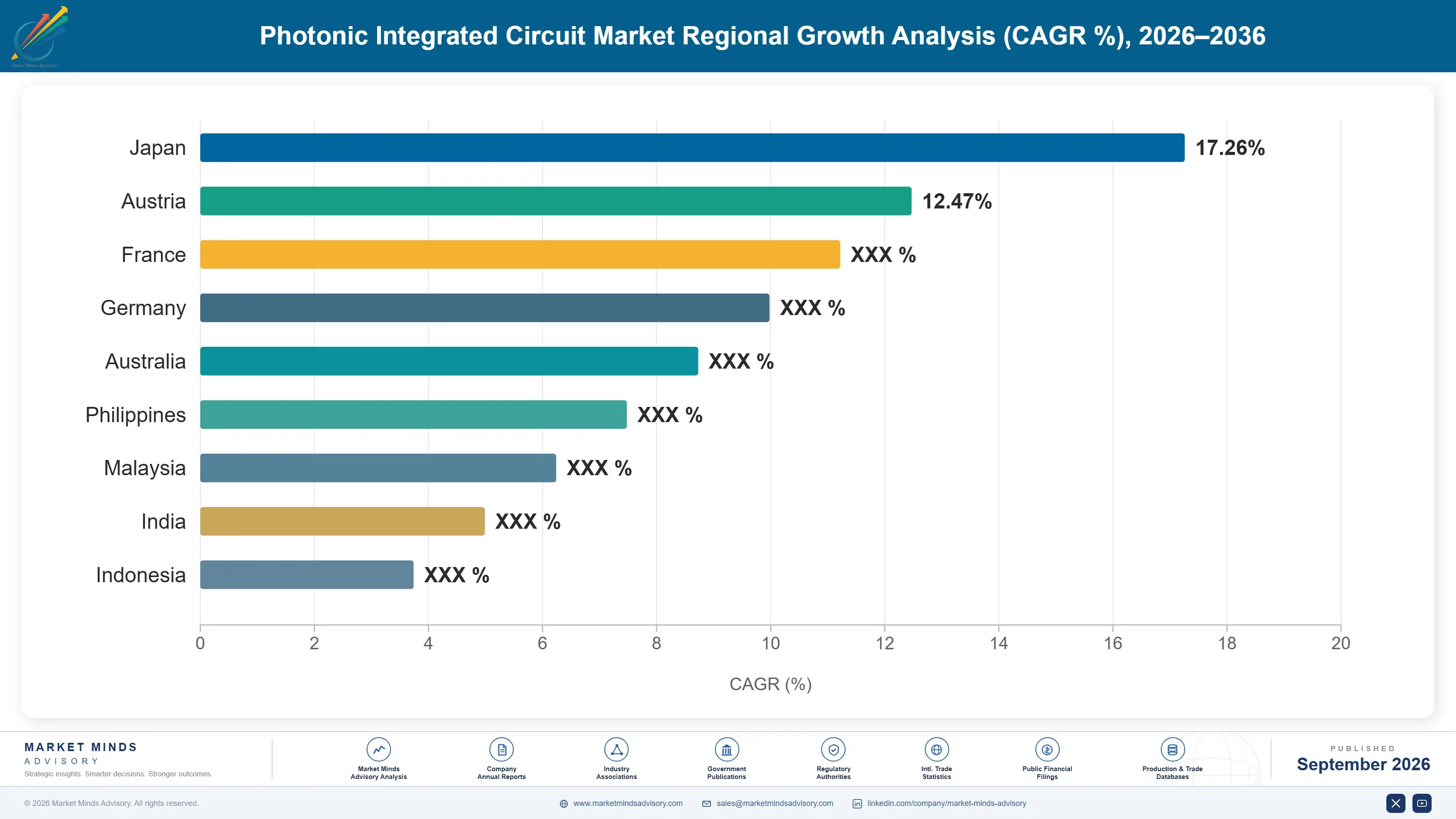
photonic-integrated-circuit-market-country-cagr-analysis-1789994977662

Where Photonic Margin Actually Sits

Packaging carries most of the cost and most of the delivery risk, design reuse is low enough that every new product generation costs close to a full price, and the fastest growing customer in this category reorders on a quarterly cadence. The four levers below follow those conditions rather than any argument about optical performance.

Own Or Contract Packaging Capacity Directly

Assembly, alignment and test account for roughly 64% of delivered device cost, so a firm designing chips and buying packaging has subcontracted the majority of its cost structure to somebody else with limited ability to improve it. Packaging capacity also queues before wafer capacity whenever demand rises, which makes it the binding delivery constraint as well as the cost one. Firms holding that capacity themselves control both of those at once. Those without it are competing on the smaller 36% of what the customer is actually paying for in the end.
Market Impact: Packaging carries fully 64% of the delivered cost

Invest In Alignment Automation Ahead Of Volume

Aligning a fibre to a waveguide within roughly 0.5 microns remains substantially manual work today, and assembly capacity therefore scales with trained people rather than with equipment that can simply be bought. Genuine throughput improvement delivers a cost position that no circuit design advantage anywhere matches, and it remains the single largest source of margin improvement available in this category. It requires capital committed well before the volume arrives, which is genuinely uncomfortable, and the firms that did it are the ones now winning data centre tenders on delivered price.
Market Impact: Alignment demands accuracy within just 0.5 microns today

Build Reusable Blocks Across Product Generations

Design reuse runs near 23% between successive product generations, because the platform physics genuinely differ and process design kits abstract only so much of that away. Every new product therefore costs close to a full development cycle, including an 11 month tape-out before evaluation. Firms building genuinely reusable circuit blocks within a single platform cut both development cost and time to market together. The obstacle here is organisational rather than technical, since design teams optimising each product individually rarely produce anything at all that the next team can actually use.
Market Impact: Design reuse currently runs at only 23% today

Serve Data Centre Buyers On Their Cadence

Data centre interconnect customers reorder quarterly and expect cost reduction on every single generation, which bears no resemblance at all to the telecom qualification cycles that this industry was originally built around. Silicon photonics for optical interconnect grows at 20.4% against 13.6% for the market as a whole, and that particular customer is where all of the volume now sits. Suppliers running telecom-paced qualification and pricing discipline lose these accounts on responsiveness rather than on product quality, and frequently do not work out why until several generations have already passed them by.
Market Impact: Interconnect compounds at fully 20.4% each year now

Who Controls the Margin Pool

Five suppliers hold 52% of photonic integrated circuit and module revenue, and vertical integration explains that concentration considerably better than fabrication capability does. Broadcom, Coherent, Lumentum, Intel and Cisco Systems lead the field on that combined basis. All participants here are assessed consistently on photonic chip and module revenue rather than on any broader semiconductor or networking business that they also happen to operate.
Competition runs on packaging cost and delivery certainty far more than on optical performance, since roughly 64% of device cost sits in assembly and that is also where orders queue. The second dimension is customer cadence, because data centre buyers reorder quarterly and expect cost reduction each generation while telecom buyers qualify slowly and then hold. Serving both of those well requires two genuinely different operating rhythms running inside a single business at once.

Pressure is emerging from specialist packaging and assembly firms selling capacity directly to chip designers who lack it, which lets fabless entrants reach volumes they otherwise simply could not. Rankings shift wherever interconnect demand concentrates rather than in telecom transport, and wherever packaging capacity has been contracted rather than merely hoped for.
photonic-integrated-circuit-market-company-positioning-matrix-1789994978184

Competitive Moat and Risk Dimensions

BROADCOM

Moat: Integrated Switch And Optics

Broadcom holds switch silicon alongside photonic capability, which matters as co-packaged optics moves the optical engine onto the switch package itself. That combination lets the company specify both halves of an interface most competitors can only supply one side of. Assembling comparable coverage requires switch silicon capability at scale, which a photonics business does not acquire quickly.
BROADCOM

Risk: Co-Packaging Timing Exposure

The advantage depends on co-packaged optics reaching volume deployment, and that transition has run behind announcements for several years already. Pluggable modules keep improving and remain easier for operators to service and replace in the field. A position built around an architectural transition is exposed to how long that transition actually takes to arrive.
COHERENT

Moat: Vertical Packaging Integration

Coherent holds materials, chip fabrication and packaging capability internally, which covers the roughly 64% of device cost that most competitors subcontract. That integration also removes the delivery constraint that catches firms depending on third-party assembly when demand rises sharply. Building comparable coverage means acquiring or constructing packaging capacity that scales with trained people rather than with equipment purchases.
COHERENT

Risk: Capital Intensity Burden

Vertical integration across materials, fabrication and packaging carries fixed cost that must be filled through demand cycles this industry has not historically delivered smoothly. Fabless competitors buying packaging capacity carry none of that burden when volumes fall. The integration that provides cost advantage in strong demand becomes an obligation when the data centre cycle turns downward.

Players Tracked

Prominent Players

Broadcom
Coherent
Lumentum
Intel
Cisco Systems

Other Key Players

Marvell Technology
Nokia Corporation
Infinera
Sumitomo Electric Industries
Fujitsu Optical Components
NeoPhotonics
Rockley Photonics
SMART Photonics
EFFECT Photonics
Hamamatsu Photonics
AMS Technologies
Jabil Photonics
Accelink Technologies
Hisense Broadband
Source Photonics

Recent Developments

JUNE 2025

Switch Vendors Extend Co-Packaged Optics Platform Development

Several switch silicon vendors extended development of co-packaged optics platforms placing optical engines onto the switch package, an engineering development rather than any merger or acquisition. That transition moves the specification decision from the network operator to the switch designer, which changes both the customer and the qualification requirements entirely.
Signal: Co-packaging moves the buying decision from the network operators across to the switch silicon designers instead.
JANUARY 2025

Photonic Packaging Capacity Expands Across Asian Assembly Sites

Assembly and test providers expanded photonic packaging capacity across Asian sites serving interconnect and telecom customers, organic capacity expansion rather than any corporate transaction. Packaging absorbs around 64% of delivered device cost and queues before wafer capacity when demand rises, making it the binding delivery constraint industry wide.
Signal: Orders queue at packaging rather than at the wafer fab, which most investment cases still miss.
SEPTEMBER 2024

Indian National Programmes Fund Photonic Design Capability

Indian national semiconductor programmes funded photonic design capability across research institutions and commercial teams, a policy development rather than any commercial transaction. Design capability is comparatively inexpensive to establish because foundry access can be purchased, whereas fabrication and packaging capacity cannot be built at anything like the same speed.
Signal: Design capability appears in countries with no manufacturing at all, because foundry access is simply purchasable.

What A Photonic Device Costs

Assembly, alignment and test absorb roughly 64% of delivered device cost, which is unusual for any semiconductor product and reflects work that remains substantially manual. Wafer fabrication takes around 17%, using existing semiconductor infrastructure in the case of silicon photonics. Specialist substrate material absorbs about 11% on indium phosphide and lithium niobate platforms, and design amortisation takes most of the remaining balance.
Thin-film lithium niobate substrate supply stayed tight through 2022 and 2023 as demand for high-speed modulation rose faster than the small producer base could serve, extending lead times considerably. Coherent Annual Report 2024 and Lumentum Annual Report 2024 both record material availability and packaging capacity as principal operating constraints. Firms holding internal packaging capacity managed the period considerably better than those depending on third-party assembly.

The competitive disadvantage mechanism is packaging access rather than material price. A firm with internal or contracted assembly capacity controls 64% of its cost and can commit to delivery dates a customer will design a product schedule around. One without it controls neither. Exposure concentrates among fabless photonic designers, whose circuit capability may be excellent while their cost and delivery position is determined entirely elsewhere.
photonic-integrated-circuit-market-cost-volatility-analysis-1789994978382

Contract Assembly Capacity Ahead Of Demand Cycles

Packaging absorbs around 64% of delivered device cost and queues before wafer capacity when demand rises sharply. Contracted assembly capacity secured ahead of the cycle lets a firm quote delivery dates that customers can build product schedules around. Firms depending on spot assembly availability cannot commit to schedule at all, which loses tenders regardless of circuit quality.

Relax Alignment Tolerance Where Applications Permit

Fibre alignment within roughly half a micron drives most of the packaging cost, and not every application genuinely requires that precision across its whole operating range. Designs tolerating looser alignment through mode expansion or on-chip coupling structures cut assembly cost directly. The engineering investment sits in the circuit rather than the factory, where photonic teams are already strongest.

Qualify Second Substrate Sources On Specialist Platforms

Indium phosphide and thin-film lithium niobate substrates run around 11% of cost and come from a very small producer base that has repeatedly been the binding supply constraint. Qualifying alternative sources costs engineering time against no immediate return and preserves delivery when the primary tightens. Firms discovering mid-shortage that nothing else is qualified have already lost the design win entirely.

Portfolio Architecture for Margin Defence

Margin architecture separates on packaging control and platform scarcity. Gallium arsenide photonic devices and standard passive circuits earn least, since the functions are established and several suppliers compete on price. Silicon nitride passive circuits sit above on process control. Silicon photonics interconnect modules, lithium niobate modulators and heterogeneous assemblies earn most, because each combines scarce platform capability with packaging complexity that few can deliver.
The volume versus premium tension runs between interconnect volume and specialist platforms, and they demand opposite operating behaviour. Interconnect moves enormous quarterly volume at compressing margin against customers who expect cost reduction every generation. Specialist platforms move modest volume at strong margin on capability few can match. Firms optimising entirely for one consistently lose their ability to serve the other properly.

High-value pools concentrate in heterogeneous integration and in packaging capability itself, and neither is reached through circuit design excellence. Heterogeneous assemblies combine platforms in ways that demand both design and assembly capability together. Packaging capacity scales with trained people rather than with capital equipment. Both take years to build, which is why the leading positions have proved so durable across successive technology transitions.

Volume / Commodity-Adjacent

Gallium arsenide photonic devices and standard passive circuits, where functions are well established and several capable suppliers compete largely on price. The ten point spread separates firms holding internal packaging capacity from those subcontracting the majority of their delivered cost.
Gross Margin: 20% to 30%

Premium / Certified

Silicon nitride passive circuits and indium phosphide active devices, where process control and material expertise determine selection alongside performance. The twelve point spread tracks substrate supply security, which varies considerably given how small the specialist producer base actually is.
Gross Margin: 34% to 46%

Sustainability / Regulatory / Next-Generation

Silicon photonics interconnect modules, lithium niobate modulator circuits and heterogeneous assemblies, combining scarce platform capability with packaging complexity that very few suppliers can deliver. The eighteen point spread reflects assembly capability more than circuit design quality.
Gross Margin: 50% to 68%
photonic-integrated-circuit-market-portfolio-architecture-1789994978881

High-value Sub-segments and Strategic Watch-out

Silicon Photonics For Optical Interconnect

Grows at fully 20.4% on data centre link demand that copper simply cannot serve at the current distances and data rates. The eighteen point spread here reflects packaging capacity control. Assembly absorbs 64% of delivered cost, so packaging rather than fabrication decides competitiveness across this segment.
Gross Margin: 50% to 68%

Lithium Niobate High-Speed Modulator Circuits

Grows at fully 17.2% because the material modulates light at bandwidths that silicon genuinely struggles to reach at current data rates. The eighteen point spread here reflects thin-film substrate access. Thin-film supply comes from a very small producer base that has repeatedly constrained delivery schedules.
Gross Margin: 50% to 68%

Indium Phosphide Active Photonic Circuits

Grows at only 11.8% on telecom transport and on specialist applications that require integrated light generation directly on the photonic circuit itself. The twelve point spread here reflects material expertise depth. Telecom weighting means considerably slower growth here than the interconnect platforms are currently achieving.
Gross Margin: 34% to 46%

Gallium Arsenide Photonic Devices

Grows at only 7.4%, the slowest of all six material platforms, on established functions where several capable suppliers compete largely on delivered price. The ten point spread here reflects packaging integration depth. Sensing and consumer applications sustain a steady volume without generating very much growth at all.
Gross Margin: 20% to 30%

Why Design Wins Persist

The annuity here is the design win rather than any supply agreement. A photonic device qualified into a product stays there for that product's life, because requalifying means a fresh tape-out cycle running around 11 months plus assembly qualification behind it. Nobody undertakes that to change supplier on price. Product lives run years in interconnect and longer in telecom, so a design win generates volume well afterwards.
Depth varies sharply by platform and by how much the customer's design depends on specific device behaviour. A heterogeneous assembly matched to a particular switch package is deeply fixed. A telecom transport device inside a qualified line system is similarly locked. A standard interconnect module meeting a published specification is far more substitutable, and data centre buyers switch between qualified suppliers on price without hesitation.

The buyer has moved from telecom equipment vendors toward hyperscale data centre operators and switch silicon designers, which changed the tempo entirely. A telecom vendor qualified slowly and then held for years. A hyperscale operator reorders quarterly and expects cost reduction every generation. A switch designer specifies co-packaged optics during silicon development. Suppliers organised around the first buyer serve the smallest and slowest part of their own market.
photonic-integrated-circuit-market-end-use-penetration-index-1789994979373

What Decides Photonic Position

These are among the four positions where our research anticipates prominent divergence between winners and laggards over the coming forecast period. Each is grounded in the demand model, the regulatory perimeter, and the announced capacity pipeline.
01 / PACKAGING CAPACITY CONTROL

Own The Sixty Four Percent

Assembly, alignment and test account for roughly 64% of delivered device cost, so a firm that designs chips and buys packaging has subcontracted the clear majority of its cost structure to somebody else with very limited ability to improve it afterwards. Packaging capacity also queues before wafer capacity whenever demand rises sharply, which makes it the delivery constraint as well as the cost one. Firms without that capacity are competing on much the smaller portion of what the customer actually pays.
02 / ALIGNMENT AUTOMATION INVESTMENT

Automate Before The Volume Arrives

Aligning a fibre to a waveguide within roughly half a micron remains substantially manual work across the industry, so assembly capacity scales with the number of trained people rather than with equipment that can simply be purchased. Genuine throughput improvement delivers a cost position that no circuit design advantage anywhere can match. It requires capital committed well before the volume arrives, and the firms that actually made that commitment are the ones now winning data centre tenders on delivered price.
03 / DESIGN BLOCK REUSE

Make The Next Generation Cheaper

Design reuse runs near 23% between successive product generations, because material platforms differ genuinely in physics and process design kits abstract only so much of that away from the designer. Every new product consequently costs close to a full development cycle, including an 11 month tape-out before anything at all can be evaluated. The obstacle is organisational rather than technical, since design teams optimising each product individually rarely leave behind anything at all that the next team can actually use.
04 / CUSTOMER CADENCE MATCHING

Run Interconnect At Quarterly Tempo

Data centre interconnect customers reorder quarterly and expect cost reduction on every generation, which bears no resemblance to the telecom qualification cycles this industry was originally built around. Silicon photonics for interconnect grows at 20.4% against 13.6% for the market, so that customer is where the volume now sits. Suppliers running telecom-paced qualification and pricing discipline lose these accounts on responsiveness rather than on any product shortcoming, and rarely work out why until several product generations have already gone past them.

Engagement Snapshot From the Field

A live engagement with an industry participant carrying material or product regulatory and market exposure ahead of a defining policy shift, showing how our research translates into a defensible multi-year portfolio strategy.
MARKET MINDS ADVISORY · CLIENT ENGAGEMENT SUMMARY
Photonic Integrated Circuit Producer Strategic Portfolio Review and Transition Roadmap 2026·Investment Scenario on Photonic Integrated Circuit Exposure Evaluation 2025-26
CLIENT PROFILE
A fabless photonic design house with strong circuit capability across silicon and silicon nitride platforms, buying both wafer fabrication and packaging from third parties. Design wins were being converted into shipped revenue far more slowly than the pipeline suggested, and the company had assumed the problem was wafer supply rather than anything happening after fabrication was complete.
STRATEGIC CHALLENGE
Engineering wanted to invest in additional circuit design capability to widen the product range. The board suspected the constraint lay elsewhere but could not identify where. Delivery had slipped on three design wins in succession, and each time the explanation offered internally had pointed at foundry scheduling rather than at anything the company itself controlled.
MMA APPROACH
MMA traced elapsed time and cost across every stage from tape-out to shipped product on the three slipped design wins, separating fabrication from assembly and test. We priced internal packaging capacity against contracted third-party alternatives, and assessed which of the client's designs could tolerate relaxed alignment. Work drew on 47 expert interviews conducted in Q4 2025 with designers, foundries and assembly providers.
KEY FINDINGS
  1. Assembly and test consumed around 7 in 10 of elapsed time from tape-out to shipment, and a comparable share of delivered cost across all three design wins.
  2. Every one of the three slipped deliveries had queued at the packaging provider rather than at the wafer foundry, which internal reporting had never separated out.
  3. Two of the designs could have tolerated substantially relaxed alignment tolerance with only modest circuit changes, cutting assembly cost meaningfully (client-reported, unverified by MMA).
  4. Contracted packaging capacity was available at a premium the company had never priced, because nobody had established what the delivery slips were actually costing.
CLIENT PROFILE
A fabless photonic design house with strong circuit capability across silicon and silicon nitride platforms, buying both wafer fabrication and packaging from third parties. Design wins were being converted into shipped revenue far more slowly than the pipeline suggested, and the company had assumed the problem was wafer supply rather than anything happening after fabrication was complete.
STRATEGIC CHALLENGE
Engineering wanted to invest in additional circuit design capability to widen the product range. The board suspected the constraint lay elsewhere but could not identify where. Delivery had slipped on three design wins in succession, and each time the explanation offered internally had pointed at foundry scheduling rather than at anything the company itself controlled.
MMA APPROACH
MMA traced elapsed time and cost across every stage from tape-out to shipped product on the three slipped design wins, separating fabrication from assembly and test. We priced internal packaging capacity against contracted third-party alternatives, and assessed which of the client's designs could tolerate relaxed alignment. Work drew on 47 expert interviews conducted in Q4 2025 with designers, foundries and assembly providers.
KEY FINDINGS
  1. Assembly and test consumed around 7 in 10 of elapsed time from tape-out to shipment, and a comparable share of delivered cost across all three design wins.
  2. Every one of the three slipped deliveries had queued at the packaging provider rather than at the wafer foundry, which internal reporting had never separated out.
  3. Two of the designs could have tolerated substantially relaxed alignment tolerance with only modest circuit changes, cutting assembly cost meaningfully (client-reported, unverified by MMA).
  4. Contracted packaging capacity was available at a premium the company had never priced, because nobody had established what the delivery slips were actually costing.
RECOMMENDED STRATEGY
Phase 1: Phase one: contract dedicated packaging capacity rather than buying assembly on spot terms, since every slipped delivery had queued there. Phase 2: Phase two: redesign the two tolerant products for relaxed alignment, which cut assembly cost without requiring any new fabrication process. Phase 3: Phase three: report elapsed time separately for fabrication and for assembly, since the combined reporting had hidden the real constraint for years.
OUTCOME
The design house contracted packaging capacity and redesigned two products for relaxed alignment tolerance (client-reported, unverified by MMA). Delivery against design wins improved measurably within three quarters. Fabrication and assembly are now tracked separately, which is the change that made the constraint visible and kept it that way.

Frequently Asked Questions

Foundational context covering the market sizes, CAGR, scope, country, region and competition that inform every finding below. This section is provided to cover basics and most often pre-purchase conversations, answered from the MMA Primary Research Dataset.

What is the current size of the Photonic Integrated Circuit Market?

Global value reaches USD 10.2 billion in 2026, measured as photonic chip and module revenue across six material platforms. The 2025 base for the market is USD 8.9 billion.

How large will the Photonic Integrated Circuit Market be by 2036?

The market reaches USD 36.5 billion by 2036, an increase of USD 26.3 billion across the forecast period. That represents 3.58 times expansion from the 2026 base.

What is the CAGR for the Photonic Integrated Circuit Market 2026 to 2036?

The base case runs at 13.6% annually, with a bull case at 14.9% if co-packaged optics reaches volume on schedule and a bear case at 12.3% if packaging capacity fails to expand alongside wafer supply.

Which segment is growing fastest?

Silicon photonics for optical interconnect grows at 20.4%, half again the market rate of 13.6%. Data centre link demand keeps rising faster than copper can carry it at current distances.

Who are the major companies in the Photonic Integrated Circuit Market?

Broadcom, Coherent, Lumentum, Intel and Cisco Systems lead on photonic chip and module revenue, together holding 52%. Marvell Technology, Infinera and Sumitomo Electric hold smaller positions.

Which country is growing fastest?

India leads at 21.7%, on photonic design capability funded through national semiconductor programmes rather than emerging commercially. China and Singapore both follow some way behind it.

Report Segmentation Architecture

The full report scope spans multiple orthogonal segmentation dimensions, with cross-tabulated demand data provided for each dimension pair. Coverage extends further to regional breakdowns, trend trajectories, and the competitive detail needed to support segment-level decision-making.

By Material Platform

  • Silicon Photonics For Optical Interconnect
  • Lithium Niobate High-Speed Modulator Circuits
  • Indium Phosphide Active Photonic Circuits
  • Silicon Nitride Passive And Low-Loss Circuits
  • Hybrid And Heterogeneously Integrated Assemblies
  • Gallium Arsenide Photonic Devices

By End-Use Industry

  • Data Centre And Cloud Interconnect
  • Telecommunications Transport Networks
  • Automotive Sensing And Ranging
  • Medical Diagnostics And Imaging
  • Industrial Instrumentation And Metrology
  • Defence And Aerospace Systems

By Commercial Dimension

  • Vertically Integrated Manufacturer Supply
  • Fabless Design With Contracted Manufacture
  • Foundry And Multi-Project Wafer Services
  • Hyperscale Operator Direct Specification
  • Switch Silicon Vendor Integration
  • Distributor And Module Channel

By Region

  • North America
  • Western Europe
  • East Asia
  • South Asia and Pacific
  • Latin America
  • Middle East and Africa
  • Eastern Europe

Scope, Methodology, and Coverage

Every figure in this report is reproducible from documented input assumptions. The scope below maps the historical period, the forecast horizon, the segmentation dimensions, and the countries covered, alongside the underlying primary and qualitative methodology.
Historical Period
2020 to 2025
Forecast Period
2026 to 2036
Base Year
2025 (USD billions; MMA Primary Research Dataset, September 2026)
Market Definition
This report covers photonic integrated circuits and the modules built from them, by material platform: silicon photonics for optical interconnect, indium phosphide active photonic circuits, silicon nitride passive and low-loss circuits, lithium niobate high-speed modulator circuits, gallium arsenide photonic devices, and hybrid and heterogeneously integrated assemblies. It excludes discrete lasers and detectors not integrated onto a photonic circuit, optical fibre and cable, passive optical components, test equipment, and complete network systems.
Quantitative Units
USD millions, chip and module revenue basis; shipped devices; packaging share of delivered cost as a percentage; fibre alignment tolerance in microns; coupling loss in decibels; tape-out cycles in months.
Segmentation Dimensions
Material platform; end-use application; commercial manufacturing and supply route; geography across seven regions.
Regions Covered
North America, Western Europe, East Asia, South Asia and Pacific, Latin America, Middle East and Africa, Eastern Europe
Countries Covered
United States, Canada, Taiwan, China, Japan, South Korea, Malaysia, Singapore, India, Australia, Netherlands, Belgium, Germany, France, United Kingdom, Poland, Czechia, Israel, Brazil, Saudi Arabia.
Key Companies Profiled
Broadcom, Coherent, Lumentum, Intel, Cisco Systems, Marvell Technology, Nokia Corporation, Infinera, Sumitomo Electric Industries, Fujitsu Optical Components, SMART Photonics, EFFECT Photonics, Hamamatsu Photonics, Accelink Technologies, Source Photonics.
Quantitative Methodology
Primary survey, n=3,800 respondents, Q4 2025, six countries; demand-side model with trade association cross-validation
Qualitative Methodology
47 expert interviews, Q4 2025; applied to validate demand model assumptions, identify emerging dynamics, and assess competitive positioning
Report Format
PDF and XLSX data workbook (Word format preview document)
Publisher
Market Minds Advisory
Report Code
MMA-2026-TEC-731
Published
September 2026
Contact
sales@marketmindsadvisory.com | www.marketmindsadvisory.com

Purchase the full Photonic Integrated Circuit Market Report (2026 to 2036).

This report sizes the global photonic integrated circuit market from 2026 to 2036 across six material platforms, six applications and seven regions. It explains why assembly, alignment and test at roughly 64% of delivered cost make packaging rather than fabrication the decisive competitive variable, and why design reuse near 23% between generations keeps development cost high on every product. The shift from telecom qualification cycles to quarterly data centre reordering is examined as an operating problem rather than a demand one. Cost composition is sourced to company annual reports. Regional analysis explains why East Asia holds 35% of value.
Six material platforms sized through to 2036
Packaging cost quantified against wafer fabrication share
Design reuse rates assessed across product generations
Twenty named suppliers assessed on photonic revenue
Four revenue levers with quantified commercial impact
Anonymised fabless design house manufacturing engagement documented fully

Built For The People Who Decide

From boardroom strategy to bench-side execution, this report is read cover-to-cover by leaders shaping the next decade of their industry, turning demand scenarios, market dynamics and valuation benchmarks into decisions.
CXOs/ Presidents/ VPs/ Managers
M&A and Corporate Development
Strategy Teams and R&D Heads
Procurement and Product Directors
Regulatory and Compliance Leaders
Investor Relations and Equity Analysts