Market Minds Advisory
Panel Level Packaging Market

Panel Level Packaging Market: Fan-Out and Heterogeneous Integration Packaging on Rectangular Panel Substrates

AI accelerator and high-performance computing demand is pushing foundries toward panel-format packaging for its larger usable area, just as automotive chipmakers adopt fan-out formats, forcing OSAT providers to prove yield parity against wafer-based methods.

Lead Analyst

Bilal Shaikh

Published

September 2026

Make Smarter Decisions with Customized Research Insights

Request a free sample report and evaluate market opportunities, growth trends, and competitive dynamics relevant to your business needs.

2025 MARKET VALUE$1.8BMarket Size 2025
2036 FORECAST VALUE$5.2BBase Case , 2026 to 2036
CAGR 2026 TO 203610.2 %Bull 11.6% / Bear 8.8%
INCREMENTAL OPPORTUNITY$3.3BNet 10- year value creation
EXPANSION MULTIPLE2.64x2036 value over 2026 base
Strategic Levers
M&A Pipeline
Regional Outlook
Country Rankings
Competitive Intelligence
Segmental Deep-dive
Call-Us : 91 93563 13602

Executive Snapshot and Market Trajectory

AI accelerator and high-performance computing demand is pushing foundries toward panel-format packaging for its larger usable area, just as automotive chipmakers adopt fan-out formats, forcing OSAT providers to prove yield parity against wafer-based methods across every production line and every qualification cycle downstream this cycle.
Heterogeneous integration panel packaging leads segment growth as hyperscale computing chipmakers phase out wafer-level formats ahead of tightening interconnect density requirements. Demand concentrates among AI accelerator and high-performance computing chipmakers, where interconnect density and thermal performance directly determine chip yield and packaging economics across every production line and qualification cycle in force today, and every allocation review a foundry eventually has to conduct across its full contracted supplier base.
Competition splits between large diversified OSAT providers supplying packaging across multiple substrate formats and smaller specialists focused on fan-out or redistribution layer engineering expertise. Tightening interconnect density requirements and rising AI chip export volume are reshaping buyer priorities, rewarding packaging providers that can document yield performance and validated thermal integrity across every fabrication facility a foundry operates, including third-party test facilities contracted to serve overflow production runs each peak allocation season across every contracted facility.
Market Definition
The panel level packaging market covers semiconductor packaging processes performed on rectangular panel substrates rather than round wafers, including fan-out, fan-in, and redistribution-layer-first formats for advanced chip integration. It excludes conventional wafer-level packaging, printed circuit board assembly, and discrete component packaging sold as standalone products.
Base Year Value
$1.8B in 2025 (MMA Primary Research Dataset, August 2026)
Forecast Period
2026 to 2036, eleven discrete annual values
CAGR
10.2% base case. Bull 11.6%. Bear 8.8%.
Fastest Growth Segment
Heterogeneous Integration Panel Packaging: 15.8% CAGR
Fastest Growth Country
Malaysia: 12.8% CAGR
Fastest Growth Region
South Asia and Pacific: 12.3% CAGR
Largest Region
East Asia: 32% of 2025 global value
Market Leaders
ASE Technology Holding Co., Ltd., Amkor Technology, Inc., JCET Group Co., Ltd., Deca Technologies, Inc., Nepes Corporation. Source: MMA Analysis based on company annual reports.
Primary Survey
n=3,800 procurement and R&D decision-makers, Q4 2025, six countries
Methodology
Demand-side build-up, cross-validated against public data, 47 expert interviews

Panel Level Packaging Market Forecast Scenarios

panel-level-packaging-market-size-forecast-scenario-1787299669908
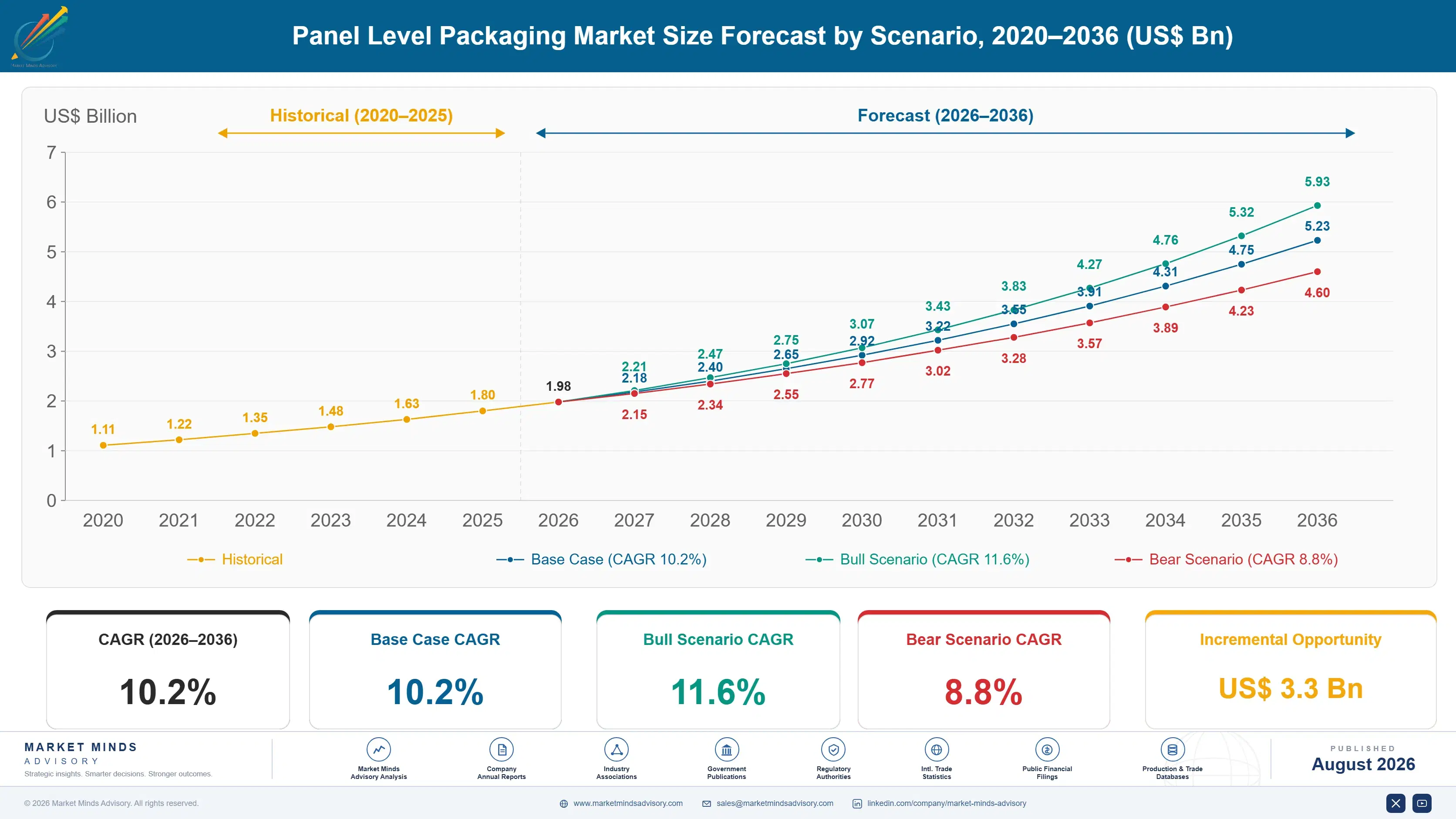
Growth from 2020 to 2025 compounded near 8.9%, restrained early by pandemic-era semiconductor supply chain disruption, then accelerating as AI accelerator demand and interconnect density requirements both expanded across multiple jurisdictions tracked over the period, particularly across East Asia and South Asia's semiconductor manufacturing sectors and their steadily tightening qualification regimes affecting standard packaging specifications nationwide.
Three mechanisms carry the base case to 10.2%. First, expanding interconnect density requirements forcing foundries to requalify packaging formats across their entire product portfolio regardless of transition cost across most affected facilities. Second, rising panel substrate economics, which favor larger usable area over round wafers given superior cost-per-chip at scale across most jurisdictions. Third, growing automotive semiconductor demand for validated thermal performance across expanding regulated chip categories and their evolving compliance requirements worldwide.
The bull case at 11.6% assumes AI accelerator demand accelerates faster than current industry forecasts suggest across major hyperscale computing markets and their foundry partners. The bear case at 8.8% assumes chipmakers delay full panel conversion as qualification timelines and yield validation persist longer than expected relative to legacy wafer-level packaging still in widespread commercial use.

AI Chip Demand Reshapes Advanced Packaging Formats

Three forces converge on panel level packaging budgets this year. Interconnect density requirements keep spreading across additional chip categories, yield certification requirements keep tightening, and foundries keep demanding documented thermal performance data before approving new packaging formats across their supply base and every fabrication contract riding on it, including third-party test facility agreements negotiated separately.
MARKET CONCENTRATIONCR5 38%top five OSAT providers hold a substantial combined revenue share
AVERAGE SELLING PRICE PREMIUM28-40% for heterogeneous formatsheterogeneous integration packaging commands a meaningful premium currently
TOP PRODUCING COUNTRY SHARETaiwan 26%leading share of global panel level packaging manufacturing capacity
CAPACITY UTILISATION74-83%panel packaging facilities running below full annual production levels
TRADE INTENSITY52%share of finished packaged chip volume crossing borders before assembly
FEEDSTOCK COST SHARE38-48%mold compound and redistribution layer materials dominate total cost
The market behaves less like a standard commodity packaging category and more like a yield economics investment wrapped around chip performance. OSAT providers compete on documented thermal performance and interconnect density depth rather than price alone, since a foundry qualifying a new packaging format faces genuine production trial and certification timelines that discourage frequent switching mid-contract, particularly once a format has been validated across a foundry's full production programme and signed off by its own quality assurance team.
Panel substrate innovation, fan-out format development, and yield certification investment are reshaping supplier selection criteria across the next decade, favoring OSAT providers that can prove consistent yield at scale against documented production baselines across comparable chip applications and their annual contract renewal cycles negotiated with major foundry accounts and their regional distribution partners nationwide.
"Foundries used to treat packaging format as a back-end afterthought behind the chip design. Now yield economics sit on the same roadmap as node transitions, and an OSAT provider that can't document panel yield parity loses the allocation before pricing even comes up."
Director, Advanced Semiconductor Packaging Practice · MMA Advanced Semiconductor

Market Trends

Fan-Out Panel Formats Replace Wafer-Level Packaging

Several major foundries have moved fan-out panel packaging beyond pilot production lines into standard specification, replacing wafer-level formats that interconnect density requirements in multiple chip categories have now made increasingly difficult to scale cost-effectively. Early deployment data across multiple foundry facilities show measurable improvements in cost-per-chip standing compared with legacy wafer-level packaging, though OSAT providers still face genuine technical tradeoffs balancing panel warpage control against yield consistency across demanding high-volume applications tracked in this year's primary survey data and expert interviews conducted across major foundry accounts and their largest fabless customer relationships.
Market Impact: Adds 11% annual conversion volume
Yield Certification Becomes a Standard Requirement

Major fabless chipmakers and foundries are pushing OSAT providers to deliver packaging validated for full yield certification, treating certification status as a procurement qualifying criterion rather than a secondary packaging feature. This shift requires OSAT providers to develop entirely new warpage control and interconnect density testing protocols separate from standard wafer-level production lines, creating a genuinely distinct product specification track that foundries increasingly treat as a yield investment rather than a simple packaging purchase decision. OSAT providers that cannot document yield certification data risk losing qualification entirely at the next contract renewal cycle.
Market Impact: Sustains packaging demand growth 14%

Market Opportunities and Growth Drivers

Expanding Interconnect Density Needs Force Format Shift

Rising interconnect density requirements across major AI and high-performance computing markets keep expanding the pool of foundries facing direct commercial incentive to switch to panel-format packaging, since fabless chipmakers cannot simply absorb rising cost-per-chip indefinitely without eventually redesigning their packaging specifications. Foundries increasingly view panel conversion as essential to managing long-term yield and cost exposure rather than discretionary process redesign, particularly across categories facing the strictest incoming interconnect density requirements and qualification deadlines this year and next across every fabrication facility. Larger foundries are moving fastest given their greater yield exposure and correspondingly higher cost at stake.
Market Impact: Limits smaller OSAT provider adoption 21%

AI Chip Export Growth Sustains Packaging Demand

Continued AI accelerator and high-performance computing export volume growth across major producing markets keeps expanding the pool of chips requiring consistent panel packaging supply, creating sustained demand independent of mature developed-market consumer electronics trends that have plateaued in North America and Western Europe. Foundries increasingly specify packaging formats with proven yield credentials rather than standard commodity grades, rewarding OSAT providers with dedicated certified product lines over those still relying entirely on generic wafer-level formulations across their broader product portfolios. This dynamic compounds each year as chip volume climbs and certification investment deepens across major foundry accounts.
Market Impact: Compresses OSAT provider margin 14%

Market Restraints and Challenges

Panel Warpage Control Strains Smaller OSAT Providers

Panel-format packaging remains meaningfully more difficult to control for warpage than conventional wafer-level formats, and smaller regional OSAT providers operating on thin capital budgets frequently cannot justify the equipment investment without confirmed yield savings to offset the higher upfront cost. The root cause is limited panel-format tooling capacity relative to mature wafer-level manufacturing infrastructure built over decades. This constrains how quickly smaller OSAT providers can convert packaging formats even when customer demand requires it, and several providers are now offering hybrid panel-wafer formulations to bridge the cost gap during the transition period and preserve margin on lower-volume accounts.
Market Impact: Raises fan-out panel share 24%

Redistribution Layer Material Supply Limits Flexibility

Redistribution layer material production remains concentrated among a limited number of specialty chemical manufacturers globally, and OSAT providers dependent on a narrow supplier base frequently cannot secure alternative sourcing quickly when disruption hits any single producer. The root cause traces to the capital-intensive dielectric material synthesis process, which few manufacturers have invested in expanding at commercial scale in recent years. This creates genuine supply risk for smaller OSAT providers, and several larger competitors are now securing dedicated material supply agreements to protect against future disruption and reduce reliance on a single feedstock source.
Market Impact: Expands certified panel packaging demand 19%
3 additional market trends, 4 additional growth drivers, and 2 additional restraints and challenges are covered in the full report. Contact sales@marketmindsadvisory.com to access the complete intelligence.

Segment CAGR and Growth Architecture

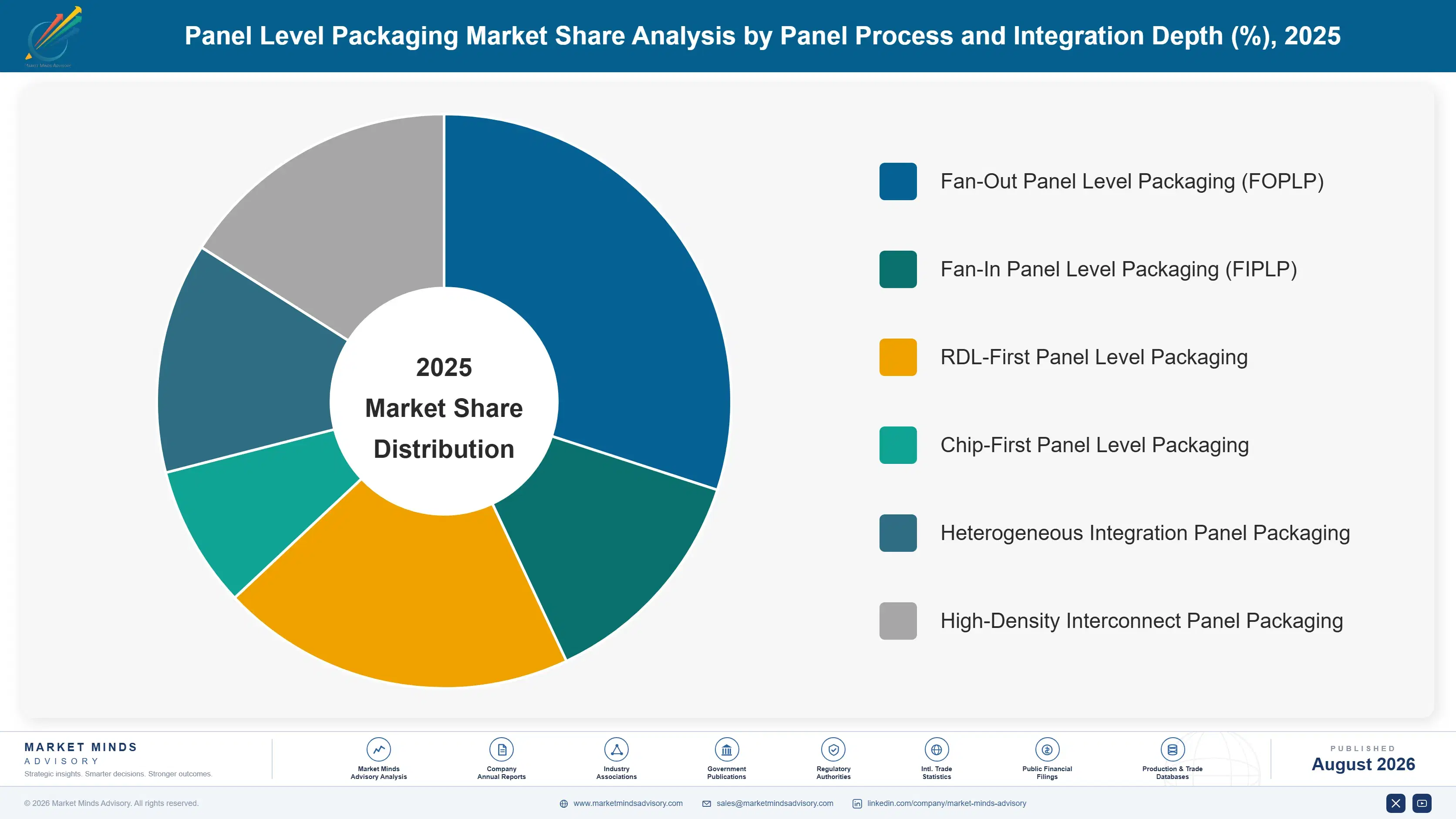
Segmentation follows panel process and integration depth because production technology, yield exposure, and foundry adoption cycles differ substantially between fan-out, fan-in, and heterogeneous categories, each carrying its own distinct OSAT capability requirement and qualification pathway shaped by chip complexity, export destination, and the buyer's own annual procurement planning cycle, freight budget, and audit calendar.
panel-level-packaging-market-market-share-analysis-1787299670442

Heterogeneous Integration Panel Packaging

This segment grows fastest at 15.8% as major AI accelerator and high-performance computing chipmakers move heterogeneous panel integration from pilot production lines into standard specification across their next-generation product programmes. OSAT providers differentiate on documented interconnect density and consistent thermal performance rather than price alone, since foundries still require extensive production trial validation before shifting primary packaging specifications away from familiar wafer-level formats. Demand concentrates among global AI accelerator and hyperscale computing chipmakers facing the strictest incoming interconnect density requirements across their largest fabrication facilities and export markets. Smaller regional foundries typically delay heterogeneous adoption until validated performance data becomes broadly available, though providers are increasingly publishing comparative studies to shorten that adoption gap for mid-size foundries too.
CAGR 15.8%

Fan-Out Panel Level Packaging (FOPLP)

Fan-out panel level packaging grows at 12.6% as chipmakers invest in scalable panel formats to reduce cost-per-chip amid intensifying competitive and cost pressure across major mobile and automotive channels. This segment carries the strongest volume-to-cost balance in the portfolio, since panel-based fan-out construction directly affects whether the finished chip meets cost and yield requirements at commercial scale. OSAT providers with advanced panel handling and high-speed redistribution capability hold a genuine advantage over competitors still relying on standard wafer-level production lacking comparable cost credentials, particularly when bidding for large multi-year foundry contracts that weigh certification depth heavily during vendor review and annual audit renewal, since qualification failures carry direct yield consequence for the buyer.
CAGR 12.6%
Full segment breakdown across 6 segments available in the complete report.

Regional Architecture and Country Demand Map

East Asia leads decisively on Taiwan and South Korea's OSAT manufacturing concentration, a share deliberately carried above the standard band given how few alternative production hubs exist, while South Asia and Pacific grows fastest as Malaysia's expanding OSAT sector scales rapidly this year and next.

North America

The United States accounts for the largest share of regional demand as major fabless chipmakers and foundries invest heavily in panel format conversion across national portfolios facing the strictest interconnect density requirements in the world. OSAT providers headquartered there, including Amkor and Deca Technologies, maintain deep foundry relationships and certification infrastructure that smaller international competitors struggle to replicate quickly. Canada contributes a smaller share tied to its own semiconductor design base, particularly across its largest provinces and their expanding research corridors. Growth outpaces the global average as ongoing AI accelerator demand keeps conversion demand elevated well above what a fully mature market would otherwise produce across every affected chip category.
Share: 23% | CAGR: 11.0% (2026 to 2036)

Western Europe

Germany and the Netherlands anchor regional demand, with both countries maintaining strict national implementation of European Union semiconductor sovereignty programmes that apply uniformly across member states regardless of individual country market size. The United Kingdom contributes steady demand through its own chip design sector investment framework supporting fabless semiconductor growth. The region's OSAT base, including SUSS MicroTec, supplies a substantial share of global panel processing equipment innovation and certification expertise, exporting proven equipment methodology to foundries elsewhere across multiple continents. Growth runs below the fastest-growing regions as the region's wafer-to-panel conversion cycle has already largely matured relative to still-transitioning markets elsewhere, leaving incremental gains concentrated in premium certified formats rather than broad volume expansion across most national jurisdictions.
Share: 19% | CAGR: 8.8% (2026 to 2036)
Regional intelligence for 5 additional markets available in the complete report: East Asia, South Asia and Pacific, Latin America, Middle East and Africa, Eastern Europe. Contact sales@marketmindsadvisory.com.
panel-level-packaging-market-country-cagr-analysis-1787299670968

Where Panel Packaging Providers Can Expand Margin

OSAT providers selling standard packaging alone are leaving margin on the table. Four levers let established providers expand revenue per foundry contract without simply chasing volume across an increasingly commoditised base wafer-level tier facing mounting price pressure from regional competitors and their aggressive spot-market pricing strategies across comparable applications and foundry client segments worldwide.

Bundle Yield Analytics and Testing Services

OSAT providers selling packaging alone leave higher-margin yield analytics and warpage testing work to internal foundry engineering teams even when the provider's own technical staff already possess the deepest knowledge of the panel's failure modes and process windows. Bundling both into a single contract raises average revenue per foundry client by an estimated 17 to 25% while reducing the customer's internal engineering burden and shortening the qualification timeline for new packaging formats considerably. Foundries increasingly prefer single-vendor accountability for both packaging supply and yield guarantees, paying a service premium for providers proving consistent uptime.
Market Impact: Raises revenue per contract 17-25% within two years

Publish Validated Panel Yield Performance Data

OSAT providers with multi-year validated yield performance data against conventional wafer-level baselines can charge premium rates over competitors offering unproven cost claims, since foundries weigh documented testing evidence heavily during vendor selection reviews tied to production continuity targets. Published performance studies covering multiple chip formats support pricing premiums of roughly 12 to 19% above standard packaging rates across comparable applications. This approach rewards providers that invested early in yield validation rather than relying on generic cost marketing claims, and it gives procurement teams a defensible basis for approving the higher unit cost internally.
Market Impact: Supports a pricing premium of roughly 12-19% overall

Secure Dedicated Redistribution Material Supply Agreements

Establishing dedicated redistribution layer material supply agreements ahead of confirmed disruption lets OSAT providers win long-term foundry contracts that competitors dependent entirely on spot-market material sourcing cannot credibly guarantee, since specialty dielectric material production remains genuinely scarce relative to expanding panel packaging demand. Early movers captured an estimated 19% larger share of new long-term supply contracts awarded over the past two years compared with providers that waited for confirmed demand signals before securing dedicated material supply agreements, since foundry buyers increasingly treat guaranteed supply continuity as a qualifying criterion rather than a bonus feature.
Market Impact: Captures roughly 19% more new supply contracts yearly

Expand Regional Panel Capacity Near Foundry Hubs

Foundries increasingly need OSAT providers positioned close to their fabrication facilities to minimize delivery lead time and support just-in-time replenishment requirements that generalist national suppliers frequently cannot supply without lengthy custom logistics arrangements across every additional manufacturing region and its seasonal peak demand swings. Providers building dedicated regional panel capacity near major foundry clusters capture incremental contract value estimated near 14% above standard national supply scope, since foundries otherwise absorb higher transport cost and lead-time risk, and providers weigh this investment against local demand density before committing capital to a new facility.
Market Impact: Adds roughly 14% incremental contract value across renewals

Who Controls the Margin Pool

CR5 sits near 38%, evaluated on disclosed panel level packaging segment revenue across public filings and industry disclosures where available. The gap between the top five diversified OSAT providers and the next tier of regional specialists is meaningful, since panel packaging requires capital-intensive equipment investment that smaller generalist competitors cannot easily replicate across every manufacturing region they serve today, leaving established leaders with durable scale advantages ove
Current competitive activity centers on three dimensions: fan-out format investment, yield certification depth, and heterogeneous integration capability. Large diversified providers bundle panel packaging into broader OSAT service contracts, while regional specialists compete purely on price and delivery proximity documented across comparable foundry deployments and their recurring renewal cycles, often winning business by outperforming generalists on a single dimension.

Emerging pressure comes from Chinese OSAT providers offering lower-cost packaging without comparable yield performance or heterogeneous integration certification, forcing established Taiwanese and Korean providers to defend premium pricing through demonstrated technical differentiation and published performance evidence. Rankings could shift toward providers combining panel innovation with sophisticated heterogeneous integration capability over the next several contract renewal cycles across major chip categories worldwide.
panel-level-packaging-market-company-positioning-matrix-1787299671489

Competitive Moat and Risk Dimensions

ASE TECHNOLOGY HOLDING CO., LTD.

Moat: Broad global OSAT manufacturing scale

ASE's massive global OSAT manufacturing scale and direct relationships with major foundries and fabless chipmakers let it bundle panel packaging into broader assembly and test contracts that regional specialists cannot match, capturing a larger share of total OSAT spend. Its established production infrastructure supports rapid qualification across new chip formats and export categories.
ASE TECHNOLOGY HOLDING CO., LTD.

Risk: Volatile semiconductor cycle exposure

ASE's substantial conventional packaging business carries meaningful exposure to semiconductor demand cycle volatility given thin margins on commodity-adjacent packaging lines, leaving profitability more sensitive to chip demand swings than competitors with more diversified OSAT portfolios able to offset softness elsewhere across unrelated categories and geographies during a prolonged industry downturn.
AMKOR TECHNOLOGY, INC.

Moat: Deep panel-level fan-out R&D investment

Amkor's sustained panel-level fan-out research investment gives it genuine formulation expertise that smaller competitors cannot easily replicate, supporting premium positioning across automotive and industrial categories requiring documented reliability evidence and rapid qualification across new foundry accounts and retail channels nationwide, reinforced by patent filings its rivals have struggled to design around.
AMKOR TECHNOLOGY, INC.

Risk: Concentrated hyperscaler customer exposure

Amkor's revenue remains concentrated across a relatively narrow set of hyperscaler and foundry customers facing capacity allocation tradeoffs during demand downturns, leaving it more exposed to customer-specific demand shifts than competitors with more diversified OSAT portfolios spanning multiple chip categories and industries across several export regions.

Players Tracked

Prominent Players

ASE Technology Holding Co., Ltd.
Amkor Technology, Inc.
JCET Group Co., Ltd.
Deca Technologies, Inc.
Nepes Corporation

Other Key Players

Powertech Technology Inc.
King Yuan Electronics Co., Ltd.
Tongfu Microelectronics Co., Ltd.
Chipbond Technology Corporation
Unisem (M) Berhad
Walton Advanced Engineering Inc.
Samsung Electro-Mechanics Co., Ltd.
Taiwan Semiconductor Manufacturing Company Limited
Applied Materials, Inc.
EV Group
SUSS MicroTec SE
BE Semiconductor Industries N.V.
ASM International N.V.
ChipMOS Technologies Inc.
Hana Micron Inc.

Recent Developments

MAY 2025

ASE launches expanded large-panel fan-out packaging platform

ASE launched an expanded large-panel fan-out packaging platform at its Taiwanese facilities, an organic capacity expansion rather than an acquisition, adding certified yield capability for foundry customers across multiple chip formats and production speeds this year and next fiscal cycle, with additional lines already planned.
Signal: Confirms established providers keep investing in panel format technology to defend premium pricing against newer regional entrants.
OCTOBER 2024

Amkor acquires regional panel-level packaging test facility

Amkor completed an acquisition of a regional panel-level packaging test facility, adding dedicated yield testing capability to its existing OSAT portfolio rather than building comparable expertise internally, extending its offering across a broader national customer base and product range spanning multiple chip categories and manufacturing regions.
Signal: Signals large diversified providers increasingly prefer acquiring specialized testing expertise over pursuing slower, costlier internal development programmes.
FEBRUARY 2025

JCET forms Southeast Asian OSAT manufacturing joint venture

JCET and a regional manufacturer formed a joint venture establishing shared panel packaging production capacity across Southeast Asian markets, splitting investment in facility buildout rather than either party expanding independently, targeting foundries seeking geographically diversified packaging supply across the broader region and its rapidly growing semiconductor assembly infrastructure.
Signal: Shows regional capacity expansion increasingly happens through shared-risk partnerships rather than solo investment this current cycle.

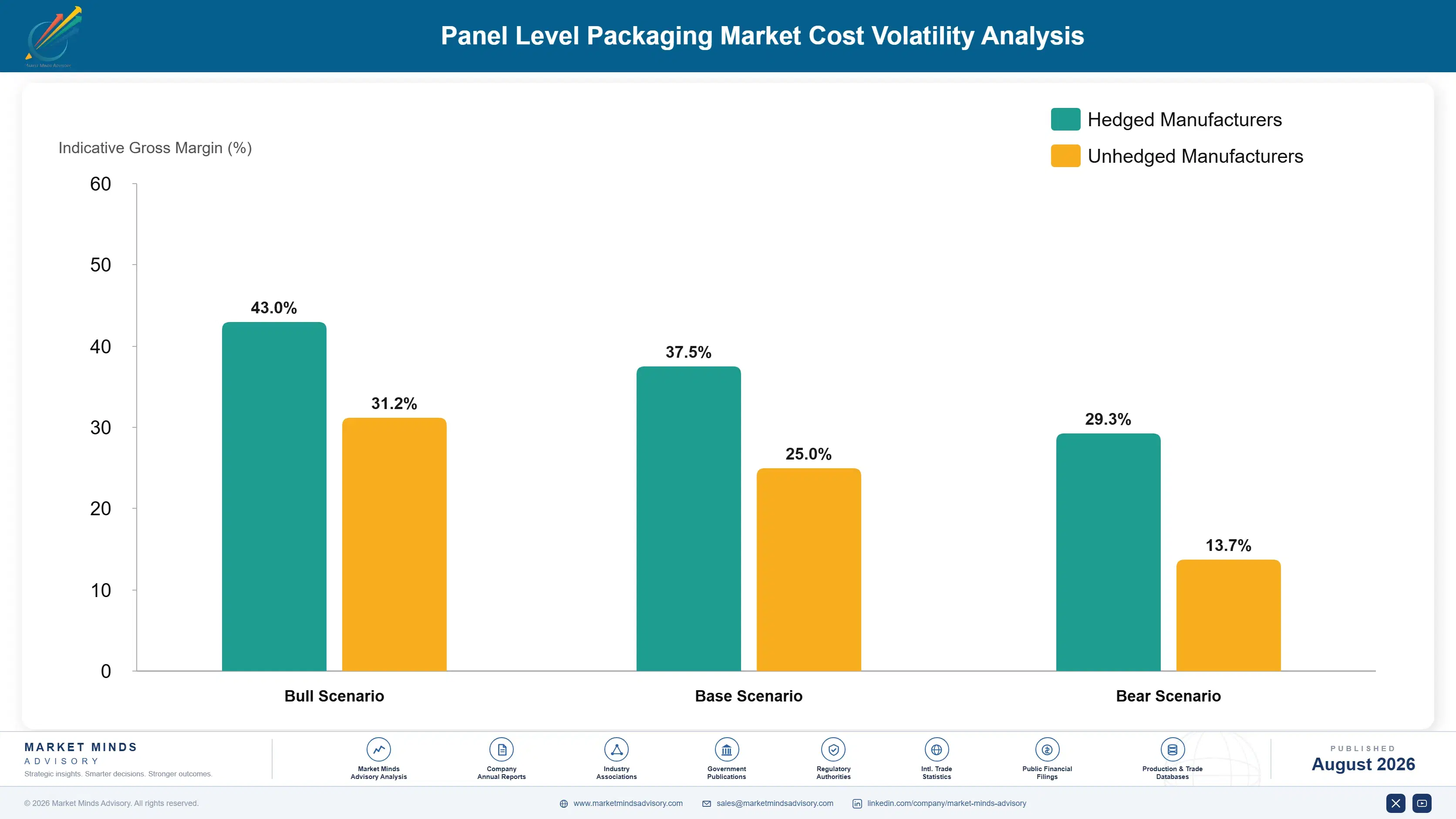
Mold Compound and Dielectric Cost Exposure

Mold compound and redistribution layer dielectric material inputs together represent roughly 38 to 48% of panel level packaging production cost, sourced primarily from specialty chemical producers concentrated across Japan, the United States, and Taiwan, where feedstock availability and production capacity both influence pricing available to downstream OSAT providers and their quoted lead times for large-volume orders placed across successive contract renewal cycles.
Global specialty resin and mold compound prices spiked significantly through 2022 as petrochemical feedstock costs surged alongside broader supply chain disruption, compressing OSAT margins across the semiconductor packaging industry, according to disclosures in ASE's annual report covering that period. Providers with multi-year fixed-price foundry contracts absorbed much of the cost increase rather than immediately repricing agreements, pressuring near-term margin significantly across affected product lines and forcing several to renegotiate terms with existing suppliers.

OSAT providers with feedstock sourcing concentrated among a small number of specialty chemical suppliers carry substantially more disruption exposure than those with diversified sourcing relationships across multiple producing regions. Smaller regional providers lacking sourcing diversification face a genuine competitive disadvantage against larger vertically integrated providers able to shift procurement toward whichever supplier currently offers the most favorable cost position.
panel-level-packaging-market-cost-volatility-analysis-1787299671684

Diversify Material Suppliers Across Regions

OSAT providers are qualifying mold compound and dielectric material suppliers across multiple producing regions rather than concentrating sourcing with a single feedstock producer, reducing single-supplier disruption exposure while maintaining flexibility to shift procurement toward whichever supplier currently offers the strongest capacity position and delivery reliability across each affected production region and its seasonal refining cycle.

Build Internal Feedstock Hedging and Contract Programmes

Larger OSAT providers are building internal feedstock hedging programmes and multi-year supply agreements specifically to smooth input cost volatility, accepting modest hedging cost in exchange for pricing predictability that spot-market purchasing cannot guarantee during genuinely volatile feedstock pricing periods affecting the broader industry and its downstream packaging operations across every major producing region and their contracted supplier base.

Index Multi-Year Contracts to Resin Price Benchmarks

Newer foundry contracts increasingly include mold compound price indexing clauses tied to published petrochemical market benchmarks, passing a portion of input cost volatility through to buyers automatically rather than absorbing the full impact against fixed multi-year pricing agreed before resin markets shifted significantly against original cost assumptions reached at the original contract signing date.

Portfolio Architecture for Margin Defence

The portfolio splits across three tiers. Volume fan-in packaging carries thin margin driven by material cost competition and regional OSAT price pressure, premium fan-out and heterogeneous formats command considerably stronger margin on certification and technical differentiation, and emerging AI-optimized closed-loop supply commands the strongest margin of all while volume remains comparatively small relative to the mature fan-in base that still anchors most provider revenue today across the in
Volume and premium work pull providers in different directions. Fan-in scale justifies continued production investment because it anchors foundry relationships and funds certification infrastructure, but margin expansion increasingly depends on winning higher-value fan-out and heterogeneous contracts layered on top of that base relationship rather than volume alone across a growing foundry roster spanning multiple chip categories and geographies.

High-value margin pools concentrate around heterogeneous integration for AI-committed foundries and validated fan-out formats serving foundries with volumes large enough to justify premium certification investment above standard fan-in rates in most established semiconductor markets with mature qualification infrastructure already in place and growing foundry willingness to pay for documented performance metrics.

Volume / Commodity-Adjacent Tier

Standard fan-in panel packaging priced on material-linked volume, competing mainly on delivery cost and regional proximity across large foundry contracts and recurring replacement orders negotiated each annual cycle across major accounts.
Gross Margin: 18-28%

Premium / Certified Tier

Fan-out and heterogeneous integration formats requiring dedicated certification infrastructure commanding higher pricing across specialist AI-committed chip categories, their renewal cycles, periodic third-party audits, and documented yield performance evidence submitted at each qualification review.
Gross Margin: 32-44%

Sustainability / Regulatory / Next-Generation Tier

AI-optimized closed-loop supply and validated advanced integration content, priced on documented performance value rather than raw volume across long-term foundry scorecard contracts, annual reporting commitments, and third-party lifecycle certification renewals covering every regulated production line.
Gross Margin: 34-46%
panel-level-packaging-market-portfolio-architecture-1787299672183

High-value Sub-segments and Strategic Watch-out

Heterogeneous Integration Panel Packaging

High value and high growth at 15.8%, the fastest category by a wide margin, as foundries move heterogeneous formats from pilot into standard specification across their next-generation programmes this year, spanning multiple chip categories and major global accounts and their export supply chains worldwide and long-term capacity plans.
Gross Margin: 34-46%

Fan-Out Panel Level Packaging (FOPLP)

High value with strong growth at 12.6%, driven by intensifying cost pressure pushing chipmakers toward more scalable panel formats across established fabrication channels and their evolving compliance requirements each renewal cycle, particularly across categories enforcing the strictest incoming yield rules and documentation standards each qualification round.
Gross Margin: 32-44%

Fan-In Panel Level Packaging (FIPLP)

The volume core by shipped units, growing near 8.8% as rising chip production volume sustains steady intake demand even as margin concentrates elsewhere across the broader portfolio, margin mix, and evolving customer specification structure tracked yearly across major foundry accounts and renewal cycles nationwide each quarter.
Gross Margin: 18-28%

RDL-First Panel Level Packaging

The strategic watch-out, growing slowest at roughly 7.0% and facing commoditisation as standard redistribution constructions become a bundled entry-level offer rather than a genuinely differentiated purchase decision across most accounts reviewed this year and last, pressuring providers to defend thinning margins and renegotiate contract terms.
Gross Margin: 19-29%

Recurring Fabrication Cycles Anchor OSAT Relationships

Panel level packaging revenue behaves like an annuity tied to each foundry's ongoing chip volume and qualification calendar rather than a one-time purchase order. Every new product launch, interconnect density requirement, and yield audit extends the OSAT relationship, and switching suppliers mid-cycle carries genuine requalification risk that keeps renewal rates high across established provider relationships built over many years of consistent performance and documented yield reliability.
Adoption depth varies considerably by foundry category. Large global AI accelerator and hyperscale computing operators facing the strictest interconnect density requirements maintain the deepest fan-out and heterogeneous format adoption given the direct commercial consequence of continued yield shortfalls, while smaller regional foundries are earlier in adopting comparable certified formats and still weighing conversion cost against yield savings. Contract assemblers sit differently, prioritizing thermal performance over pure cost messaging in most current specifications.

A generational shift is underway in foundry procurement leadership. Younger process engineers trained on advanced integration methodology favor providers demonstrating documented yield performance over providers relying purely on established reputation, gradually reshaping which suppliers win new long-term packaging mandates across the industry and its largest accounts each renewal cycle.
panel-level-packaging-market-end-use-penetration-index-1787299672670

Priorities for Panel Packaging Providers

These are among the four positions where our research anticipates prominent divergence between winners and laggards over the coming forecast period. Each is grounded in the demand model, the regulatory perimeter, and the announced capacity pipeline.
01 / HETEROGENEOUS FORMAT INVESTMENT

Fund heterogeneous capacity before competitors close the gap

OSAT providers without validated heterogeneous integration technology will lose ground to competitors that invested early, since foundries increasingly demand documented yield evidence before signing new supply contracts across qualification-exposed accounts. The window for differentiated positioning is narrowing as more providers reach comparable technical maturity within the next several contract renewal cycles. Waiting another budget cycle risks permanent competitive disadvantage against early movers who already hold demonstrable performance evidence in front of prospective foundry clients, particularly across the largest accounts now finalizing next year's supplier shortlists.
02 / REDISTRIBUTION MATERIAL SUPPLY SECURITY

Secure dedicated material supply to guarantee reliability

Foundries increasingly demand supply security that spot-market material sourcing alone cannot guarantee, making dedicated redistribution material supply agreements a genuine competitive advantage rather than optional procurement spending. Providers investing now secure premium contract positioning that competitors relying purely on spot-market sourcing will struggle to match. Waiting for confirmed demand leaves providers bidding for whatever capacity remains after earlier movers have already secured it, a gap that widens further as demand pressure expands and material capacity investment remains slow to materialize across most producing regions.
03 / YIELD CERTIFICATION ENGINEERING

Invest in certification capability to capture demand

Yield certification gaps continue excluding providers from foundry contracts that would otherwise convert given sufficient technical confidence, representing substantial unmet demand that providers investing in certification engineering can capture ahead of competitors. Providers that delay this investment risk losing the eventual panel conversion wave entirely to competitors already positioned with proven certified formulations. This engineering work compounds over successive production cycles, so providers that start now widen their advantage against slower competitors with each passing year, particularly as foundries standardize on fewer approved vendors.
04 / REGIONAL CAPACITY EXPANSION

Expand capacity near fast-growing semiconductor markets

South Asia and East Asia's expanding semiconductor assembly demand represents substantial first-time conversion demand that providers lacking regional presence cannot fully capture given established foundry preference for geographically proximate suppliers. Expanding capacity now captures share before competitors establish comparable regional footholds. Providers that delay this investment risk losing first-mover advantage entirely to regional competitors already building local foundry relationships and distribution networks across these expanding markets, and once those relationships harden into multi-year contracts the opening for a new entrant narrows considerably.

Engagement Snapshot From the Field

A live engagement with an industry participant carrying material or product regulatory and market exposure ahead of a defining policy shift, showing how our research translates into a defensible multi-year portfolio strategy.
MARKET MINDS ADVISORY · CLIENT ENGAGEMENT SUMMARY
Panel Level Packaging Producer Strategic Portfolio Review and Transition Roadmap 2026·Investment Scenario on Panel Level Packaging Exposure Evaluation 2025-26
CLIENT PROFILE
A national AI accelerator fabless chipmaker running multiple product lines across several foundry partnerships engaged MMA while evaluating whether to convert its entire packaging portfolio to panel formats ahead of an approaching next-generation node transition. The client reported facing projected annual yield loss and cost-per-chip exposure exceeding 4.8 million dollars under its current wafer-level packaging mix (client-reported, unverified by MMA).
STRATEGIC CHALLENGE
The client's existing wafer-level packaging could not meet new interconnect density thresholds taking effect across several major product lines, yet full portfolio conversion risked disrupting yield performance across dozens of chip formats simultaneously. Leadership needed a defensible conversion plan before the next product launch window, with limited internal packaging engineering resources available to build one independently.
MMA APPROACH
MMA benchmarked the client's full product portfolio against interconnect density thresholds, modeled three conversion scenarios spanning full immediate conversion, phased conversion, and selective high-exposure conversion, and evaluated four OSAT provider candidates against certification capability, yield performance data, and disclosed pricing benchmarks drawn from comparable recent engagements across similar product portfolios and their documented conversion timelines.
KEY FINDINGS
  1. Only two of four evaluated providers offered validated panel packaging performance meeting the client's strictest yield requirements without requiring additional independent third-party testing beforehand.
  2. A phased conversion prioritizing the highest-density-exposure product lines first matched the approach used by three comparable chipmakers reviewed during this engagement's benchmarking exercise.
  3. Full immediate conversion across the entire portfolio would have required simultaneous reformulation trials across dozens of chip formats, creating unacceptable near-term operational risk.
  4. Selective conversion of the highest-volume product lines captured 65% of projected yield savings while requiring only 37% of the total conversion investment needed.
CLIENT PROFILE
A national AI accelerator fabless chipmaker running multiple product lines across several foundry partnerships engaged MMA while evaluating whether to convert its entire packaging portfolio to panel formats ahead of an approaching next-generation node transition. The client reported facing projected annual yield loss and cost-per-chip exposure exceeding 4.8 million dollars under its current wafer-level packaging mix (client-reported, unverified by MMA).
STRATEGIC CHALLENGE
The client's existing wafer-level packaging could not meet new interconnect density thresholds taking effect across several major product lines, yet full portfolio conversion risked disrupting yield performance across dozens of chip formats simultaneously. Leadership needed a defensible conversion plan before the next product launch window, with limited internal packaging engineering resources available to build one independently.
MMA APPROACH
MMA benchmarked the client's full product portfolio against interconnect density thresholds, modeled three conversion scenarios spanning full immediate conversion, phased conversion, and selective high-exposure conversion, and evaluated four OSAT provider candidates against certification capability, yield performance data, and disclosed pricing benchmarks drawn from comparable recent engagements across similar product portfolios and their documented conversion timelines.
KEY FINDINGS
  1. Only two of four evaluated providers offered validated panel packaging performance meeting the client's strictest yield requirements without requiring additional independent third-party testing beforehand.
  2. A phased conversion prioritizing the highest-density-exposure product lines first matched the approach used by three comparable chipmakers reviewed during this engagement's benchmarking exercise.
  3. Full immediate conversion across the entire portfolio would have required simultaneous reformulation trials across dozens of chip formats, creating unacceptable near-term operational risk.
  4. Selective conversion of the highest-volume product lines captured 65% of projected yield savings while requiring only 37% of the total conversion investment needed.
RECOMMENDED STRATEGY
Phase 1: Phase 1 (Months 1-4): Convert the highest-density-exposure product lines to certified panel packaging immediately and reliably across every leading facility. Phase 2: Phase 2 (Months 5-9): Extend conversion to remaining high-volume product lines while monitoring yield performance closely throughout each successive run. Phase 3: Phase 3 (Months 10-15): Evaluate yield savings achieved and plan final portfolio conversion based on documented performance data collected across phases.
OUTCOME
The client adopted the phased conversion plan and reported a 58% reduction in projected yield loss and cost-per-chip exposure within the first year, while avoiding operational disruption across its highest-volume product lines and preserving existing foundry relationships throughout the full fifteen-month conversion window across every affected facility (client-reported, unverified by MMA).

Frequently Asked Questions

Foundational context covering the market sizes, CAGR, scope, country, region and competition that inform every finding below. This section is provided to cover basics and most often pre-purchase conversations, answered from the MMA Primary Research Dataset.

What is the current size of the Panel Level Packaging Market?

The global panel level packaging market is valued at USD 1.8 billion in 2025, covering fan-out, fan-in, and heterogeneous integration packaging performed on rectangular panel substrates.

How large will the Panel Level Packaging Market be by 2036?

The market is projected to reach USD 5.24 billion by 2036, roughly 2.64 times its 2026 value of USD 1.98 billion, driven by AI accelerator demand and interconnect density requirements.

What is the CAGR for the Panel Level Packaging Market 2026 to 2036?

The base case CAGR is 10.2%, with a bull case of 11.6% if AI accelerator demand accelerates faster than expected, and a bear case of 8.8% under slower conversion.

Which segment is growing fastest?

Heterogeneous Integration Panel Packaging leads at a 15.8% CAGR, roughly 1.55 times the overall market rate, as foundries move heterogeneous formats into standard specification across next-generation AI accelerator programmes.

Who are the major companies in the Panel Level Packaging Market?

ASE Technology, Amkor, JCET, Deca Technologies, and Nepes lead the market, together holding roughly 38% of panel packaging segment revenue generated worldwide, per company filings.

Which country is growing fastest?

Malaysia leads at a 12.8% CAGR as its rapidly expanding OSAT sector scales domestic panel packaging capacity across a growing semiconductor assembly consumer base and export corridors.

Report Segmentation Architecture

The full report scope spans multiple orthogonal segmentation dimensions, with cross-tabulated demand data provided for each dimension pair. Coverage extends further to regional breakdowns, trend trajectories, and the competitive detail needed to support segment-level decision-making.

By Panel Process and Integration Depth

  • Fan-Out Panel Level Packaging (FOPLP)
  • Fan-In Panel Level Packaging (FIPLP)
  • RDL-First Panel Level Packaging
  • Chip-First Panel Level Packaging
  • Heterogeneous Integration Panel Packaging
  • High-Density Interconnect Panel Packaging

By End-Use Application

  • AI Accelerator and High-Performance Computing
  • Mobile and Consumer Electronics
  • Automotive Semiconductor Packaging
  • Industrial and IoT Semiconductor Packaging
  • Networking and Data Center Chips

By Commercial Dimension

  • Direct Foundry Assembly Contracts
  • Fabless Chipmaker Outsourcing Agreements
  • Equipment and Process Licensing Channels
  • Regional Contract Assembly Partnerships

By Region

  • North America
  • Western Europe
  • East Asia
  • South Asia and Pacific
  • Latin America
  • Middle East and Africa
  • Eastern Europe

Scope, Methodology, and Coverage

Every figure in this report is reproducible from documented input assumptions. The scope below maps the historical period, the forecast horizon, the segmentation dimensions, and the countries covered, alongside the underlying primary and qualitative methodology.
Historical Period
2020 to 2025
Forecast Period
2026 to 2036
Base Year
2025 (USD billions; MMA Primary Research Dataset, August 2026)
Market Definition
The panel level packaging market covers semiconductor packaging processes performed on rectangular panel substrates rather than round wafers, including fan-out, fan-in, and redistribution-layer-first formats for advanced chip integration. It excludes conventional wafer-level packaging, printed circuit board assembly, and discrete component packaging sold as standalone products.
Quantitative Units
USD billions (current prices); panel volume in unit counts where applicable
Segmentation Dimensions
By Panel Process and Integration Depth; By End-Use Application; By Commercial Dimension; By Region
Regions Covered
North America, Western Europe, East Asia, South Asia and Pacific, Latin America, Middle East and Africa, Eastern Europe
Countries Covered
Taiwan, South Korea, China, USA, Germany, Netherlands, UK, Japan, Malaysia, India, Australia, Canada, Brazil, Mexico, Saudi Arabia, UAE, South Africa, Poland, Hungary, Romania, and additional markets relevant to this sector
Key Companies Profiled
ASE Technology Holding Co., Ltd., Amkor Technology, Inc., JCET Group Co., Ltd., Deca Technologies, Inc., Nepes Corporation, Powertech Technology Inc., King Yuan Electronics Co., Ltd., Tongfu Microelectronics Co., Ltd., Chipbond Technology Corporation, Unisem (M) Berhad, Walton Advanced Engineering Inc., Samsung Electro-Mechanics Co., Ltd., Taiwan Semiconductor Manufacturing Company Limited, Applied Materials, Inc., EV Group, SUSS MicroTec SE, BE Semiconductor Industries N.V., ASM International N.V., ChipMOS Technologies Inc., Hana Micron Inc.
Quantitative Methodology
Primary survey, n=3,800 respondents, Q4 2025, six countries; demand-side model with trade association cross-validation
Qualitative Methodology
47 expert interviews, Q4 2025; applied to validate demand model assumptions, identify emerging dynamics, and assess competitive positioning
Report Format
PDF and XLSX data workbook (Word format preview document)
Publisher
Market Minds Advisory
Report Code
MMA-2026-TEC-100
Published
August 2026
Contact
sales@marketmindsadvisory.com | www.marketmindsadvisory.com

Purchase the full Panel Level Packaging Market Report (2026 to 2036).

The full report delivers granular sizing and forecasts across all six panel process segments and seven global regions through 2036, with dedicated analysis of Taiwan and South Korea's OSAT concentration. It profiles twenty companies across diversified OSAT providers and specialist panel packaging equipment makers, benchmarking fan-out coverage, yield certification depth, and material supply security in considerable detail. Analysts detail feedstock cost exposure, portfolio margin tiers, and demand architecture by foundry category across major global markets. Buyers receive both the standalone report and full access to underlying data tables supporting every figure and forecast presented throughout.
Six-segment panel process sizing and full forecasts
Seven-region global market share breakdown detail
Twenty-company detailed competitive profile benchmarking analysis
Feedstock cost exposure and mitigation pathway analysis
Portfolio margin tier benchmarking economics framework
Anonymised client engagement outcome case study

Built For The People Who Decide

From boardroom strategy to bench-side execution, this report is read cover-to-cover by leaders shaping the next decade of their industry, turning demand scenarios, market dynamics and valuation benchmarks into decisions.
CXOs/ Presidents/ VPs/ Managers
M&A and Corporate Development
Strategy Teams and R&D Heads
Procurement and Product Directors
Regulatory and Compliance Leaders
Investor Relations and Equity Analysts