Market Minds Advisory
Non-UV Dicing Tapes Market

Non-UV Dicing Tapes Market: Adhesion Balance, Thin Wafer Handling and the Consumable That Decides Die Yield

A tape must grip a wafer hard enough that no die shifts during sawing, then release each one without cracking it, and getting that balance wrong destroys silicon worth thousands of times the tape itself.

Lead Analyst

Bilal Shaikh

Published

September 2026

Make Smarter Decisions with Customized Research Insights

Request a free sample report and evaluate market opportunities, growth trends, and competitive dynamics relevant to your business needs.

2025 MARKET VALUE$0.7BMarket Size 2025
2036 FORECAST VALUE$1.7BBase Case , 2026 to 2036
CAGR 2026 TO 20368.8 %Bull 10.0% / Bear 7.6%
INCREMENTAL OPPORTUNITY$1.0BNet 10- year value creation
EXPANSION MULTIPLE2.32x2036 value over 2026 base
Strategic Levers
M&A Pipeline
Regional Outlook
Country Rankings
Competitive Intelligence
Segmental Deep-dive
Call-Us : 91 93563 13602

Executive Snapshot and Market Trajectory

Dicing tape costs a few dollars per wafer and the wafer costs thousands. That ratio is why nobody in semiconductor assembly buys this consumable on price, and why a tape qualified into a process line is almost never displaced by a cheaper equivalent. Nobody buys this consumable on price.
Thin wafer and ultra-thin die tapes compound at 13.2%, exactly 1.50 times the market, as memory stacking and power devices push wafers below 50 micrometres where handling damage becomes the dominant yield loss. East Asia holds 58% of demand, far above any normal regional band, because semiconductor assembly and test capacity is concentrated there to a degree no other materials market matches. Yield is the whole argument.
Five suppliers hold 71%, which is high even for semiconductor consumables. Adhesive formulation is the barrier: a tape must hold every die immovable during sawing then release it undamaged, and that balance is qualified per device, per saw and per die size. Nobody requalifies to save a few dollars. Qualification runs 26 weeks and covers the tape, the saw, the blade, the die size and the pick-up sequence as one interacting system.
Market Definition
The market covers pressure-sensitive tapes used to mount semiconductor wafers during dicing and singulation where die release is achieved without ultraviolet curing, spanning standard non-UV dicing tapes, thin wafer and ultra-thin die tapes, back-grinding and dicing combination tapes, high-temperature and laser-compatible tapes, die attach film backing tapes and compound semiconductor dicing tapes. Ultraviolet-curable dicing tapes, wafer carrier films and dicing equipment are excluded.
Base Year Value
$0.7B in 2025 (MMA Primary Research Dataset, August 2026)
Forecast Period
2026 to 2036, eleven discrete annual values
CAGR
8.8% base case. Bull 10.0%. Bear 7.6%.
Fastest Growth Segment
Thin Wafer and Ultra-Thin Die Tapes: 13.2% CAGR
Fastest Growth Country
India: 12.4% CAGR
Fastest Growth Region
South Asia and Pacific: 11.0% CAGR
Largest Region
East Asia: 58% of 2025 global value
Market Leaders
Nitto Denko, Lintec Corporation, Furukawa Electric, Denka, Mitsui Chemicals. Source: MMA Analysis based on company annual reports.
Primary Survey
n=3,800 procurement and R&D decision-makers, Q4 2025, six countries
Methodology
Demand-side build-up, cross-validated against public data, 47 expert interviews

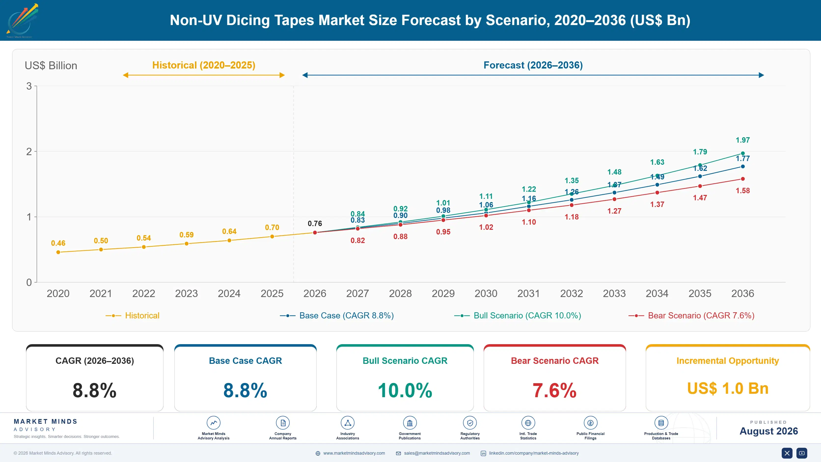
Non-UV Dicing Tapes Market Forecast Scenarios

non-uv-dicing-tapes-market-size-forecast-scenario-1787307944743
Growth ran at an implied 7.4% across 2020 to 2025 and it tracked semiconductor unit volume rather than semiconductor revenue, which diverged sharply through the period. The 2021 shortage drove assembly capacity hard, then the 2023 memory downturn cut wafer starts substantially while advanced packaging volumes continued rising throughout. Unit volume and revenue told different stories.
The base case at 8.8% rests on three mechanisms. Wafer thinning continues as memory stacking and power devices demand die below 50 micrometres, and thin wafers need tapes that conventional formulations cannot serve. Advanced packaging multiplies the number of singulation steps per finished device. And silicon carbide and gallium nitride devices require tapes that survive harder, more abrasive sawing than silicon ever demanded. All three mechanisms add tape consumption independently of wafer starts, which is unusual for a semiconductor consumable.
The bull case at 10.0% assumes advanced packaging adoption accelerates further, since each additional stacking or reconstitution step adds a separate tape consumption event. The bear case at 7.6% follows from ultraviolet-curable tapes taking share in applications where clean release matters more than thermal tolerance, which would erode the non-ultraviolet position in exactly the growing thin-die segment.

Two Contradictory Jobs in One Adhesive

Dicing tape has to do two things that directly contradict each other. During sawing it must hold every die absolutely immobile, because a die that shifts by a few micrometres meets the blade wrongly and chips. Immediately afterwards it must let each die go without applying enough force to crack it. The adhesive has to be strong and then weak, and the transition has to happen on command.
TOP FIVE CONCENTRATION71%Combined share held by the five largest global suppliers
TAPE COST AGAINST WAFER0.3% of valueConsumable cost as proportion of the silicon it carries
QUALIFICATION CYCLE26 weeksTypical time to qualify a tape into production
THIN WAFER THRESHOLD50 micrometresThickness below which conventional tape formulations stop performing
DIE LOSS FROM HANDLING62% of defectsShare of singulation yield loss attributable to mounting and release
ASSEMBLY CAPACITY CONCENTRATION81% in regionProportion of global assembly and test capacity in one geography
Ultraviolet-curable tapes solve this by dropping adhesion sharply when exposed to light. Non-ultraviolet tapes achieve the transition through formulation and through the mechanics of expansion and pick-up instead, which makes them essential wherever ultraviolet exposure would damage the device, wherever the process runs hot, or wherever an additional cure step cannot be accommodated on the line. That protected core cannot be contested.
The economics are lopsided in a way that governs everything. The tape represents around 0.3% of the value of the silicon it carries, while 62% of singulation yield loss traces back to mounting and release. Buying this consumable on price is irrational, and semiconductor assembly operations behave accordingly, treating a 26 week qualification as the real cost of any change.
"I have never once heard an assembly manager complain that dicing tape was expensive. What I hear about constantly is a tape that released a batch of thin die badly on a Thursday afternoon, and how many months it will take to qualify a replacement."
Director, Semiconductor Materials and Advanced Packaging Practice · MMA Semicond

Market Trends

Wafer Thinning Below Fifty Micrometres Breaks Conventional Formulations

Memory stacking, power devices and fingerprint sensors all require die thinned well below 50 micrometres, and at that thickness silicon behaves more like a membrane than a plate. Conventional tape adhesion that worked perfectly on a 200 micrometre wafer cracks a 30 micrometre die during pick-up, because the release force exceeds what the silicon can absorb. Thin wafer tapes use adhesive systems engineered for a far lower and more uniform release force. The segment compounds at 13.2% against a market at 8.8%, and conventional grades simply cannot substitute. Qualification is device-specific throughout.
Market Impact: Compound devices at 17% of demand

Advanced Packaging Multiplies Singulation Steps Per Device

A conventionally packaged chip is diced once. A device using fan-out wafer level packaging, chiplet integration or die stacking passes through singulation several times: the original wafer, the reconstituted panel, and sometimes the finished module. Each pass consumes tape. That multiplication means dicing tape demand grows faster than wafer starts, which is unusual for a semiconductor consumable and is the principal reason category growth held up through the 2023 memory downturn when wafer volumes fell sharply. That is why category growth held up through the 2023 memory downturn when wafer volumes fell sharply across the industry.
Market Impact: Protected core covering 29% of volu

Market Opportunities and Growth Drivers

Compound Semiconductors Demand Tapes Silicon Never Required

Silicon carbide and gallium nitride are considerably harder than silicon and generate more heat and debris during sawing, which loads the tape differently. Laser and plasma singulation, used increasingly for these materials, applies thermal stress that softens conventional adhesives and contaminates the die surface. Power electronics for electric vehicles and industrial drives have driven compound semiconductor volumes up sharply. Roughly 17% of non-ultraviolet tape demand now serves compound devices, and those grades price well above silicon equivalents because the formulation problem is harder. Formulation difficulty rather than volume sets the price.
Market Impact: Ultraviolet taking 4 points annuall

Ultraviolet Exposure Damages an Expanding Set of Devices

Image sensors, certain memory structures and some micro-electromechanical devices are damaged or shifted by the ultraviolet dose that curable tapes require for release, which rules those tapes out entirely regardless of their other advantages. The population of ultraviolet-sensitive devices has grown as sensor integration spread through automotive, mobile and industrial applications. Non-ultraviolet formulations are the only option in those processes, which gives the category a protected core that ultraviolet competition cannot reach at any price. Sensor integration keeps widening that pool rather than holding it steady, so the protected core is growing alongside the contested one.
Market Impact: Qualification adding 26 week delays

Market Restraints and Challenges

Ultraviolet-Curable Tapes Offer Cleaner Release on Thin Die

Ultraviolet curing drops adhesion by an order of magnitude on command, which delivers a lower and more predictable pick-up force than formulation alone achieves. The root cause is physical: a chemical crosslinking event is simply more controllable than a mechanical release balance. On very thin die that difference matters, and ultraviolet tapes have taken share in applications where the device tolerates the exposure. Suppliers mitigate by developing low-release non-ultraviolet grades and by concentrating on ultraviolet-sensitive devices and high-temperature processes where no substitution exists. The physical advantage cannot be fully closed.
Market Impact: Thin die tapes compounding at 13.2%

Qualification Cycles Delay Revenue From New Formulations

A new tape takes around 26 weeks to qualify into a production process, and considerably longer to displace an incumbent already running. The root cause is that qualification covers tape, saw, blade, die size and pick-up equipment as an interacting system, so nothing transfers cleanly between customers. That makes formulation development expensive to monetise and slow to scale. Suppliers mitigate by qualifying platform adhesive systems across multiple device families upfront and by co-developing with equipment makers before customers evaluate. Nothing transfers cleanly between customers. Formulation development is expensive to monetise as a result.
Market Impact: Advanced packages using 3 tape pass
3 additional market trends, 4 additional growth drivers, and 2 additional restraints and challenges are covered in the full report. Contact sales@marketmindsadvisory.com to access the complete intelligence.

Segment CAGR and Growth Architecture

Segmentation follows tape functional type, because the release requirement, thermal tolerance and backing construction differ completely between them. A thin die tape and a high-temperature laser dicing tape solve unrelated problems using different adhesive chemistry, and no single formulation serves both applications acceptably. A supplier credible in one is not automatically credible in another.
non-uv-dicing-tapes-market-market-share-analysis-1787307945276

Thin Wafer and Ultra-Thin Die Tapes

Thin wafer tapes compound at 13.2%, exactly 1.50 times the market rate, because silicon below 50 micrometres behaves in ways conventional tape was never designed for. At that thickness a die flexes rather than resisting, and the release force that lifted a 200 micrometre die cleanly will crack a 30 micrometre one. These tapes use adhesive systems delivering a much lower and far more uniform pick-up force, with backing films engineered for controlled expansion so die spacing opens evenly across the frame. Memory stacking, power devices and sensor integration all drive the requirement. Conventional grades cannot substitute at any price, and qualification is device-specific enough that positions persist for a product generation.
CAGR 13.2%

High-Temperature and Laser-Compatible Tapes

High-temperature grades grow at 11.6% on singulation methods that generate far more thermal load than a mechanical blade does. Laser grooving, stealth dicing and plasma singulation all deposit energy into the tape as well as the wafer, and a conventional adhesive softens, outgasses or leaves residue on the die surface under that load. Compound semiconductors compound the problem, since silicon carbide and gallium nitride demand more aggressive singulation than silicon. These tapes use adhesive and backing chemistry with genuinely different thermal stability, they cost meaningfully more, and the field of suppliers able to formulate them credibly is narrower than in any other part of the category. Pricing reflects that scarcity directly.
CAGR 11.6%
Full segment breakdown across 6 segments available in the complete report.

Regional Architecture and Country Demand Map

Demand sits where wafers are diced, which is not where they are fabricated and certainly not where finished devices are consumed. Semiconductor assembly and test capacity is more geographically concentrated than almost any other manufacturing activity of comparable value. Assembly geography rather than device consumption is the map worth reading.

East Asia

East Asia holds 58% of global demand. Note: this is far outside the standard regional band because semiconductor assembly and test capacity is concentrated in Taiwan, China, South Korea and Japan to a degree matched by no other manufacturing activity, and dicing tape is consumed where wafers are singulated rather than where devices are designed or used. Taiwanese outsourced assembly and test providers account for the single largest share, and Chinese assembly capacity has expanded rapidly under domestic semiconductor investment programmes. Japanese demand is smaller in volume but sets the technical standard, and all five leading suppliers are Japanese. Korean memory stacking drives thin wafer tape consumption specifically. Growth of 9.4% tracks assembly capacity addition and packaging adoption.
Share: 58% | CAGR: 9.4% (2026 to 2036)

South Asia and Pacific

South Asia and Pacific accounts for 14% of demand and grows fastest at 11.0%, with India compounding at 12.4%. Note: this share also exceeds the standard band, reflecting Malaysian, Singaporean and Philippine assembly and test capacity that has served the industry for decades alongside newer Indian investment. Malaysia in particular hosts substantial outsourced assembly operations serving global device makers. Indian assembly and test investment under national semiconductor programmes is early but growing quickly from essentially nothing, and every new facility qualifies tape suppliers from scratch, which is an unusual commercial opportunity in a category where positions normally persist. Australian demand is negligible. Vietnamese assembly capacity has expanded as manufacturing relocated from China.
Share: 14% | CAGR: 11.0% (2026 to 2036)
Regional intelligence for 5 additional markets available in the complete report: North America, Western Europe, Latin America, Middle East and Africa, Eastern Europe. Contact sales@marketmindsadvisory.com.
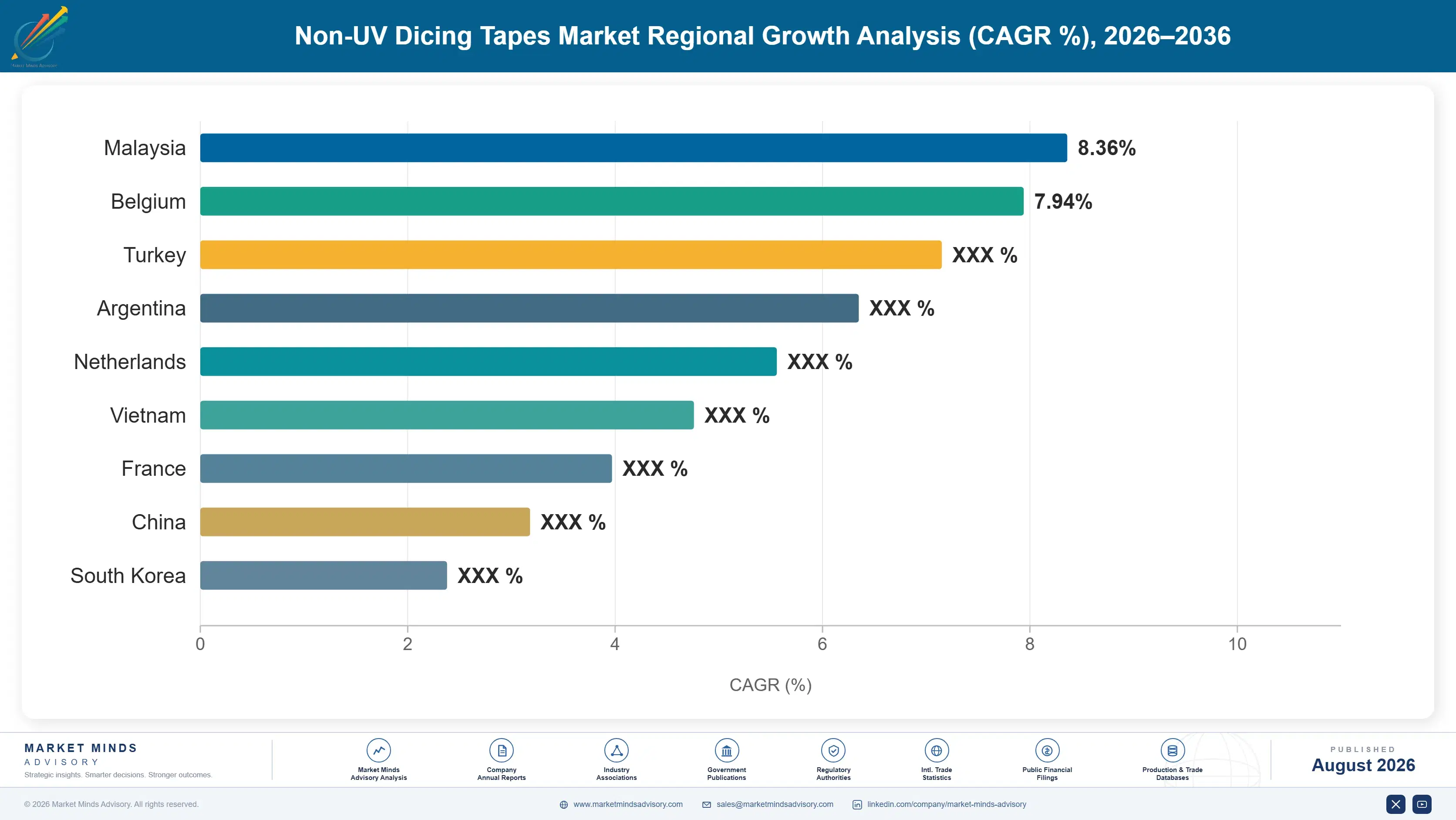
non-uv-dicing-tapes-market-country-cagr-analysis-1787307945797

Where a Cheap Consumable Earns Real Margin

Nothing here is won on price, because the tape is 0.3% of the silicon it carries and a bad release destroys the rest. What decides business is whether a supplier can solve a handling problem the customer has not solved, and get qualified before a competitor does. Four positions follow from that. Price is never the variable.

Formulate for Die Thinner Than Fifty Micrometres

Below 50 micrometres silicon flexes rather than resisting, and the release force that lifted a thick die cleanly cracks a thin one. Conventional grades cannot substitute at any price, which is why thin wafer tapes compound at 13.2% against a market at 8.8%. Adhesive systems delivering low and highly uniform pick-up force, with backing films engineered for controlled expansion, are the requirement. Gross margins run roughly 14 to 21 points above standard grades, and qualification is device-specific enough that a won position typically holds for an entire product generation. Substitution is not available.
Market Impact: Thin die grades carrying 14 to 21 p

Qualify Ahead of New Assembly Capacity Coming Online

A tape takes around 26 weeks to qualify and far longer to displace an incumbent, which makes an existing line almost closed to a new supplier. New assembly capacity is the exception: a greenfield facility qualifies everything from scratch with no incumbent to displace. Indian, North American and Chinese assembly investment is creating those openings now, and suppliers engaging during equipment installation rather than after production start capture positions that will hold for a decade. The commercial requirement is knowing where capacity is being built before it is commissioned. Timing beats relationship depth here.
Market Impact: Greenfield lines qualifying inside

Own the Ultraviolet-Sensitive Device Applications Entirely

Image sensors, certain memory structures and some micro-electromechanical devices are damaged by the ultraviolet dose curable tapes require, which excludes those tapes entirely regardless of their release advantages. That protected core covers roughly 29% of non-ultraviolet volume and cannot be competed for on performance grounds at all. Sensor integration keeps spreading through automotive, mobile and industrial devices, so the pool is growing rather than static. Concentrating development on these applications avoids competing against a physically superior release mechanism in the segments where it genuinely wins. Physics does the defending here.
Market Impact: Protected applications at 29% of th

Build Thermal Tolerance for Compound Semiconductor Singulation

Silicon carbide and gallium nitride demand more aggressive singulation than silicon, and laser grooving, stealth dicing and plasma methods all deposit energy into the tape. Conventional adhesives soften, outgas or leave residue on the die surface under that load. Compound devices already represent 17% of non-ultraviolet demand and grow with electric vehicle power electronics. The adhesive and backing chemistry required is genuinely different, the supplier field able to formulate it is narrower than anywhere else in the category, and pricing reflects both facts consistently. Very few can formulate it credibly.
Market Impact: Compound work at 17% of all current

Who Controls the Margin Pool

Five suppliers hold 71% of the market measured on dicing tape revenue, the basis applied consistently through this section. Concentration is high even for semiconductor consumables, and all five are Japanese, which reflects decades of adhesive formulation depth built alongside a domestic semiconductor industry. Nitto Denko and Lintec Corporation lead clearly. Scale confers little against formulation depth here.
Competition operates on three dimensions. Adhesive formulation capability decides whether a supplier can solve a customer's specific handling problem at all. Qualification position decides who is already inside a running line, which is close to unassailable. And co-development relationships with dicing equipment makers decide who reaches a new process before customers begin evaluating tape at all. All three are built over years rather than bought.

Two pressures will move rankings. Korean and Chinese suppliers have improved substantially and compete credibly on standard grades in their home assembly markets. Against that, thin die and compound semiconductor applications reward formulation depth that newer entrants have not yet built. Rankings will shift toward whoever qualifies fastest into the assembly capacity being constructed now. Very few are positioned for both today.
non-uv-dicing-tapes-market-company-positioning-matrix-1787307946318

Competitive Moat and Risk Dimensions

NITTO DENKO

Moat: Adhesive formulation depth

Nitto Denko's position rests on decades of pressure-sensitive adhesive development spanning far more than semiconductor applications, which gives it formulation options when a customer presents an unusual release or thermal requirement. That breadth matters because dicing tape problems are rarely solved by adjusting an existing grade, and the company can reach across a much wider chemistry portfolio than specialists hold.
NITTO DENKO

Risk: Ultraviolet substitution exposure

Ultraviolet curing delivers a lower and more predictable pick-up force than formulation alone can achieve, which matters increasingly as die get thinner and the growth concentrates there. Where a device tolerates the exposure, ultraviolet tapes hold a genuine physical advantage that no amount of adhesive development fully closes, and that segment is expanding rather than shrinking.
LINTEC CORPORATION

Moat: Integrated back-grinding and dicing

Lintec supplies back-grinding tape, dicing tape and die attach film as a connected system, which matters for thin wafers where the same piece of silicon passes through grinding, mounting and pick-up without ever becoming self-supporting. Controlling the full handling chain lets the company solve problems that arise at the interfaces between steps, which a single-product supplier cannot address at all.
LINTEC CORPORATION

Risk: Concentration in Japanese customers

A customer base weighted toward Japanese device makers and their overseas operations limits participation in the Chinese and Indian assembly capacity growing fastest. Those facilities qualify suppliers from scratch, which is precisely the rare opening in a category where positions otherwise persist, and competitors closer to those customers commercially are better placed to take them.

Players Tracked

Prominent Players

Nitto Denko
Lintec Corporation
Furukawa Electric
Denka
Mitsui Chemicals

Other Key Players

Sumitomo Bakelite
AI Technology
Ultron Systems
Loadpoint
Pantech Tape
Shin-Etsu Chemical
Sekisui Chemical
Maxell
Dongguan Kaiyue Adhesive Products
Hitachi Chemical Techno Service
Nagase and Co
3M
Achem Technology
Shanghai Rightway Tape
Sanwa Kako

Recent Developments

JANUARY 2025

Memory stacking drives thin wafer tape qualification programmes

Memory manufacturers extended high-bandwidth stacking capacity, requiring die thinned well below 50 micrometres and prompting qualification of tapes engineered for far lower pick-up force. These were process qualification activities rather than corporate transactions, and conventional grades were excluded on technical grounds. Release force rather than adhesion strength decided the outcome.
Signal: Below fifty micrometres the tape choice st
MAY 2025

Compound semiconductor singulation expands high-temperature tape demand

Silicon carbide device manufacturers increased use of laser and plasma singulation methods that deposit substantially more thermal energy into the mounting tape than blade sawing does. This reflects process adoption rather than any acquisition, and it excludes conventional adhesive systems from those lines entirely. Conventional adhesive systems were excluded.
Signal: The singulation method rather than the dev
SEPTEMBER 2025

New assembly capacity creates rare supplier qualification openings

Semiconductor assembly and test facilities under construction across India, China and North America began qualifying consumable suppliers ahead of production start, with no incumbent tape position to displace. These were greenfield commissioning activities rather than commercial transactions between suppliers. Suppliers engaging during installation reached those evaluations first.
Signal: A greenfield line is the only realistic en

Films, Adhesives and Cleanroom Conversion

Backing film accounts for roughly 26% of cost of goods, principally polyolefin and polyvinyl chloride grades manufactured to tight thickness and cleanliness specifications. Adhesive raw materials including acrylic monomers, tackifiers and crosslinkers run a further 24%. Cleanroom conversion, slitting and packaging carry disproportionate cost because particulate contamination on a dicing tape becomes a defect on a die.
Acrylic monomer and speciality tackifier pricing moved sharply through 2022 and 2023 as European energy disruption raised petrochemical intermediate costs, and International Energy Agency reporting across that period documents the underlying movement. Semiconductor consumable suppliers absorbed much of it, because a qualified tape cannot be reformulated to a cheaper input without triggering the 26 week requalification the customer will not accept. Company annual reports covering electronic materials segments disclose the resulting margin pressure.

Exposure divides by qualification depth rather than by scale. A supplier holding qualified positions on running lines cannot change formulation to manage cost, so input increases flow straight to margin until contracts renew. One selling standard grades into less demanding applications has more formulation freedom but faces regional competitors with lower cost bases. Cleanroom conversion cost is the common burden and it scales poorly at low volume.
non-uv-dicing-tapes-market-cost-volatility-analysis-1787307946516

Dual-source adhesive raw materials before qualification

A qualified tape cannot switch raw material source without requalification, so the time to secure a second supply route is during development rather than after a customer position exists. Qualifying two monomer or tackifier sources within one formulation costs one additional development cycle and removes an exposure that becomes permanent the moment a customer qualifies the product.

Negotiate indexation into multi-year consumable agreements

Semiconductor customers value supply continuity above price and will generally accept raw material indexation when it is separated from the qualified specification. Framing input cost as a pass-through distinct from the tape itself avoids any suggestion the product might change. Suppliers raising this before a cost movement fare considerably better than those raising it after.

Concentrate cleanroom conversion at high-utilisation sites

Cleanroom conversion and slitting carry high fixed cost and scale poorly below full utilisation, and particulate control requirements make a marginal facility expensive to operate. Consolidating conversion at fewer higher-utilisation sites reduces unit cost materially, though it lengthens supply routes into assembly regions that value short lead times highly. Lead time into assembly regions lengthens as a consequence.

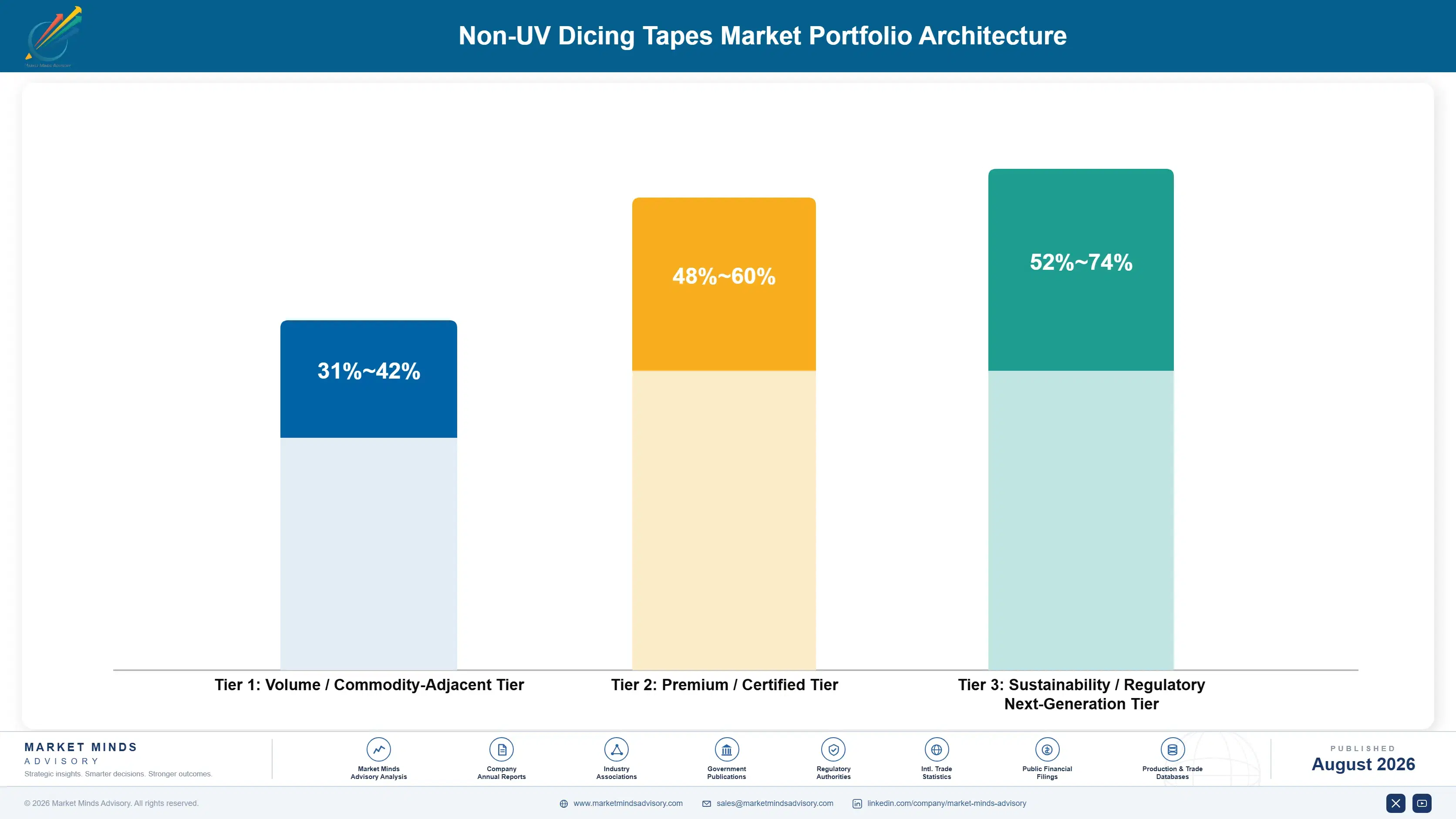
Portfolio Architecture for Margin Defence

The portfolio separates on whether a handling problem exists that the customer cannot solve otherwise. Standard grades for conventional silicon at conventional thickness face competition from Korean, Chinese and Taiwanese suppliers, and margins reflect that. Thin die, high-temperature and compound semiconductor grades solve problems where no substitute performs, and pricing follows the absence of alternatives rather than any cost basis. Substitutability draws the whole ladder here. Nothing about
The tension is that standard grades carry the volume and the customer relationships from which specialist qualification opportunities emerge. A supplier that withdraws from conventional applications loses visibility at the assembly operations where thin die programmes eventually start. Most successful participants hold standard positions deliberately as access and treat the specialist grades as where margin is actually earned. Access and margin are separate objectives. Standard positions are bought as visibility rather than as profit.

High-value pools concentrate where physics rather than preference sets the requirement. Die below 50 micrometres, laser and plasma singulation, and ultraviolet-sensitive devices all qualify, and none of them can be served by a supplier without genuine formulation capability. Formulation capability is the common requirement. None of them tolerates a supplier without it.

Volume / Commodity-Adjacent Tier

Standard non-ultraviolet dicing tapes for conventional silicon at conventional thickness, running on blade saws in mature assembly processes. Korean, Chinese and Taiwanese suppliers compete credibly here, and qualification barriers are lower than elsewhere in the category.
Gross Margin: 31-42%

Premium / Certified Tier

Thin wafer and ultra-thin die tapes, back-grinding and dicing combination products, and die attach film backing tapes requiring engineered release force and controlled expansion behaviour that conventional formulations cannot deliver.
Gross Margin: 48-60%

Sustainability / Regulatory / Next-Generation Tier

High-temperature and laser-compatible tapes plus compound semiconductor grades for silicon carbide and gallium nitride singulation. The wide margin range reflects the gap between established laser grades and newer compound formulations still being qualified.
Gross Margin: 52-74%
non-uv-dicing-tapes-market-portfolio-architecture-1787307947018

High-value Sub-segments and Strategic Watch-out

Ultra-Thin Die Handling Tapes

Compounding at 13.2% because silicon below 50 micrometres flexes rather than resisting, and conventional release force cracks it during pick-up. No substitution exists at any price, and device-specific qualification means a won position typically holds for a full product generation. Memory stacking keeps driving it.
Gross Margin: 50-62%

High-Temperature Laser Dicing Tapes

Growing at 11.6% as laser grooving, stealth dicing and plasma singulation deposit energy that softens conventional adhesives or leaves residue on the die. The formulation field is narrower here than anywhere else in the category, and pricing reflects that consistently. Compound devices compound the requirement.
Gross Margin: 56-74%

Standard Silicon Dicing Tapes

The volume core at 6.4%, contested by Korean, Chinese and Taiwanese suppliers in their home assembly markets. Run for customer visibility and conversion utilisation rather than margin, since specialist opportunities emerge from existing relationships at the same sites. Withdrawing costs the visibility. Relationships start here.
Gross Margin: 31-42%

Ultraviolet Substitution Exposure

The watch-out. Ultraviolet curing delivers a lower and more predictable release force than formulation achieves, and it is taking roughly four points of share annually in thin die applications where devices tolerate the exposure involved. Formulation alone cannot close that gap. Application selection is the only real defence.
Gross Margin: 28-52%

Qualified Once, Supplied for Years

This is among the stickiest consumable positions in any industry. A tape qualified into a production line, against a specific saw, blade, die size and pick-up sequence, is supplied for as long as that device is manufactured, because requalification takes 26 weeks and risks yield on a product already shipping. The customer bears the switching cost entirely, which is why the tape being 0.3% of wafer value never becomes a procurement conversation. Switching cost sits entirely with the customer.
Depth varies by device type rather than by customer size. Memory and sensor manufacturers running thin die buy deepest, involving suppliers in development before a process exists. Power semiconductor makers buy deeply on thermal specification. Mature logic and discrete assembly buys standard grades and tenders periodically. Outsourced assembly providers sit between, qualifying to whatever their device customer specifies.

The specifying population has moved upstream. Tape used to be selected by the assembly process engineer once a line was running. Increasingly it is chosen during device and package development, alongside the singulation method, which means a supplier absent from that conversation never reaches the evaluation at all. Reaching that conversation is now the commercial problem.
non-uv-dicing-tapes-market-end-use-penetration-index-1787307947506

Where Tape Suppliers Actually Compete

These are among the four positions where our research anticipates prominent divergence between winners and laggards over the coming forecast period. Each is grounded in the demand model, the regulatory perimeter, and the announced capacity pipeline.
01 / THIN DIE FORMULATION

Below fifty micrometres, conventional tape simply stops working

Silicon thinned past 50 micrometres flexes rather than resisting, and the release force that lifted a thick die cleanly will crack a thin one during pick-up. Conventional grades cannot substitute at any price, which is why thin wafer tapes compound at 13.2% against a market at 8.8%. Adhesive systems delivering low and highly uniform pick-up force with controlled backing expansion carry margins 14 to 21 points above standard grades, and a won position typically holds for a full product generation.
02 / GREENFIELD QUALIFICATION TIMING

New assembly capacity is the only realistic way into a running category

Qualification takes around 26 weeks and displacing an established incumbent takes very much longer, which makes an operating production line effectively closed to any new supplier entirely. Greenfield facilities are the one exception, since they qualify every consumable from scratch with no incumbent position at all to displace. Assembly investment across India, China and North America is creating exactly those openings now, and suppliers engaging during equipment installation rather than after production start win positions that then hold for a decade.
03 / ULTRAVIOLET IMMUNITY POSITIONING

Sell where the competing technology is physically excluded

Image sensors, certain memory structures and some micro-electromechanical devices are damaged outright by the ultraviolet dose that curable tapes require for release, which rules those products out of the process entirely, whatever their other advantages. That protected core covers roughly 29% of all non-ultraviolet volume and simply cannot be contested on performance grounds at any price whatsoever. Sensor integration keeps spreading through automotive, mobile and industrial devices alike, so that protected pool is expanding steadily rather than merely holding its existing position.
04 / SINGULATION THERMAL LOAD

The cutting method now sets the specification, not the device

Laser grooving, stealth dicing and plasma singulation each deposit energy into the mounting tape as well as into the wafer, and conventional adhesives soften, outgas or leave residue on the die surface under that load. Silicon carbide and gallium nitride demand exactly those singulation methods, and compound devices already represent roughly 17% of all non-ultraviolet tape demand. The adhesive and backing chemistry required is genuinely different from standard grades, and very few suppliers anywhere in the world can formulate it credibly.

Engagement Snapshot From the Field

A live engagement with an industry participant carrying material or product regulatory and market exposure ahead of a defining policy shift, showing how our research translates into a defensible multi-year portfolio strategy.
MARKET MINDS ADVISORY · CLIENT ENGAGEMENT SUMMARY
Non-UV Dicing Tapes Producer Strategic Portfolio Review and Transition Roadmap 2026·Investment Scenario on Non-UV Dicing Tapes Exposure Evaluation 2025-26
CLIENT PROFILE
An assembly and test provider operating eleven facilities across East and Southeast Asia, processing roughly 2.4 million wafers annually (client-reported, unverified by MMA). Dicing tape spend ran near USD 31 million (client-reported, unverified by MMA) across four qualified suppliers, with qualification decisions historically made facility by facility rather than at group level. No group-level view of tape performance existed at all.
STRATEGIC CHALLENGE
Die loss during singulation had risen as customers moved to thinner wafers, and two large device customers had raised yield concerns formally. Procurement proposed consolidating tape suppliers to secure better pricing. The process engineering group argued that the yield problem was a formulation mismatch and that consolidating on price would make it considerably worse.
MMA APPROACH
MMA analysed singulation yield loss by die thickness, tape grade and facility across eighteen months of production data, separating mounting and release failures from saw and blade causes. Supplier formulation capability was assessed against the thin die roadmaps the client's own customers had shared, and qualification timelines were mapped against planned capacity additions.
KEY FINDINGS
  1. Die loss correlated almost entirely with wafer thickness rather than with tape supplier, and losses rose sharply below 60 micrometres regardless of which of the four qualified grades was being used at the time.
  2. None of the four qualified suppliers had a thin die grade running at the client, though three offered one, because no facility had connected the yield data to tape specification.
  3. Two new facilities under construction would qualify consumables from scratch, and the client had not planned tape qualification into the commissioning schedule at all.
  4. Tape spend represented under 0.3% of the silicon value processed, so the pricing consolidation under discussion could not have offset even a fraction of the yield loss being incurred.
CLIENT PROFILE
An assembly and test provider operating eleven facilities across East and Southeast Asia, processing roughly 2.4 million wafers annually (client-reported, unverified by MMA). Dicing tape spend ran near USD 31 million (client-reported, unverified by MMA) across four qualified suppliers, with qualification decisions historically made facility by facility rather than at group level. No group-level view of tape performance existed at all.
STRATEGIC CHALLENGE
Die loss during singulation had risen as customers moved to thinner wafers, and two large device customers had raised yield concerns formally. Procurement proposed consolidating tape suppliers to secure better pricing. The process engineering group argued that the yield problem was a formulation mismatch and that consolidating on price would make it considerably worse.
MMA APPROACH
MMA analysed singulation yield loss by die thickness, tape grade and facility across eighteen months of production data, separating mounting and release failures from saw and blade causes. Supplier formulation capability was assessed against the thin die roadmaps the client's own customers had shared, and qualification timelines were mapped against planned capacity additions.
KEY FINDINGS
  1. Die loss correlated almost entirely with wafer thickness rather than with tape supplier, and losses rose sharply below 60 micrometres regardless of which of the four qualified grades was being used at the time.
  2. None of the four qualified suppliers had a thin die grade running at the client, though three offered one, because no facility had connected the yield data to tape specification.
  3. Two new facilities under construction would qualify consumables from scratch, and the client had not planned tape qualification into the commissioning schedule at all.
  4. Tape spend represented under 0.3% of the silicon value processed, so the pricing consolidation under discussion could not have offset even a fraction of the yield loss being incurred.
RECOMMENDED STRATEGY
Phase 1: Phase 1 (months 1 to 7): Qualify thin die grades from two existing suppliers at the three facilities handling the highest volumes below 60 micrometres. Phase 2: Phase 2 (months 7 to 16): Build tape qualification into the commissioning schedule for both new facilities rather than qualifying after production start. Phase 3: Phase 3 (months 16 to 28): Move qualification decisions to group level with process engineering rather than procurement holding the specification.
OUTCOME
Singulation yield loss on sub-60 micrometre die fell by roughly 38% within a year of the first thin die qualification (client-reported, unverified by MMA), worth approximately USD 24 million in recovered silicon value against a tape spend increase near USD 4 million. Both customers withdrew their formal yield concerns (client-reported, unverified by MMA).

Frequently Asked Questions

Foundational context covering the market sizes, CAGR, scope, country, region and competition that inform every finding below. This section is provided to cover basics and most often pre-purchase conversations, answered from the MMA Primary Research Dataset.

What is the current size of the Non-UV Dicing Tapes Market?

The global market was worth USD 0.68 billion in 2025, reaching USD 0.74 billion in 2026. East Asia holds the largest regional share at 58% of demand.

How large will the Non-UV Dicing Tapes Market be by 2036?

MMA forecasts USD 1.71 billion by 2036, an expansion multiple of 2.32 times the 2026 base. That represents roughly USD 0.97 billion of incremental value.

What is the CAGR for the Non-UV Dicing Tapes Market 2026 to 2036?

The base case compounds at 8.8% annually, with a bull case of 10.0% and a bear case of 7.6%. Historical growth from 2020 to 2025 ran at 7.4%.

Which segment is growing fastest?

Thin wafer and ultra-thin die tapes compound at 13.2%, exactly 1.50 times the market rate. Silicon below 50 micrometres flexes rather than resisting, and conventional release force cracks it.

Who are the major companies in the Non-UV Dicing Tapes Market?

Nitto Denko, Lintec Corporation, Furukawa Electric, Denka and Mitsui Chemicals hold a combined 71% of the market. All five are Japanese, reflecting decades of adhesive formulation depth.

Which country is growing fastest?

India compounds at 12.4%, ahead of every other national market. Assembly and test investment under national semiconductor programmes is building capacity up from essentially nothing.

Report Segmentation Architecture

The full report scope spans multiple orthogonal segmentation dimensions, with cross-tabulated demand data provided for each dimension pair. Coverage extends further to regional breakdowns, trend trajectories, and the competitive detail needed to support segment-level decision-making.

By Tape Functional Type

  • Standard Non-UV Dicing Tapes
  • Thin Wafer and Ultra-Thin Die Tapes
  • Back-Grinding and Dicing Combination Tapes
  • High-Temperature and Laser-Compatible Tapes
  • Die Attach Film Backing Tapes
  • Compound Semiconductor Dicing Tapes

By End-Use Industry

  • Memory and Storage Devices
  • Logic and Processor Devices
  • Power Semiconductors and Discretes
  • Image Sensors and Optoelectronics
  • Micro-Electromechanical Systems

By Commercial Dimension

  • Direct Supply to Device Manufacturers
  • Outsourced Assembly and Test Supply
  • Distributor and Regional Agent Channel
  • Co-Development With Equipment Makers

By Region

  • North America
  • Western Europe
  • East Asia
  • South Asia and Pacific
  • Latin America
  • Middle East and Africa
  • Eastern Europe

Scope, Methodology, and Coverage

Every figure in this report is reproducible from documented input assumptions. The scope below maps the historical period, the forecast horizon, the segmentation dimensions, and the countries covered, alongside the underlying primary and qualitative methodology.
Historical Period
2020 to 2025
Forecast Period
2026 to 2036
Base Year
2025 (USD billions; MMA Primary Research Dataset, August 2026)
Market Definition
The market covers pressure-sensitive tapes used to mount semiconductor wafers during dicing and singulation where die release is achieved without ultraviolet curing, spanning standard non-ultraviolet dicing tapes, thin wafer and ultra-thin die tapes, back-grinding and dicing combination tapes, high-temperature and laser-compatible grades, die attach film backing tapes and compound semiconductor dicing tapes. Ultraviolet-curable dicing tapes, wafer carrier and support films used outside singulation, dicing frames, saw blades and singulation equipment are excluded. Sizing is measured at supplier revenue in current prices.
Quantitative Units
USD billions (current prices); square metres of tape and wafers mounted where applicable
Segmentation Dimensions
By Tape Functional Type; By End-Use Industry; By Commercial Dimension; By Region
Regions Covered
North America, Western Europe, East Asia, South Asia and Pacific, Latin America, Middle East and Africa, Eastern Europe
Countries Covered
USA, China, Germany, France, UK, Japan, South Korea, India, Australia, Canada, Brazil, Mexico, Indonesia, Vietnam, Thailand, Malaysia, UAE, Saudi Arabia, South Africa, Nigeria, Turkey, Poland, Netherlands, Italy, Spain, Sweden, Switzerland, Argentina, Colombia, Singapore, and additional markets relevant to this sector
Key Companies Profiled
Nitto Denko, Lintec Corporation, Furukawa Electric, Denka, Mitsui Chemicals, Sumitomo Bakelite, AI Technology, Ultron Systems, Loadpoint, Pantech Tape, Shin-Etsu Chemical, Sekisui Chemical, Maxell, Dongguan Kaiyue Adhesive Products, Hitachi Chemical Techno Service, Nagase and Co, 3M, Achem Technology, Shanghai Rightway Tape, Sanwa Kako
Quantitative Methodology
Primary survey, n=3,800 respondents, Q4 2025, six countries; demand-side model with trade association cross-validation
Qualitative Methodology
47 expert interviews, Q4 2025; applied to validate demand model assumptions, identify emerging dynamics, and assess competitive positioning
Report Format
PDF and XLSX data workbook (Word format preview document)
Publisher
Market Minds Advisory
Report Code
MMA-2026-TEC-703
Published
August 2026
Contact
sales@marketmindsadvisory.com | www.marketmindsadvisory.com

Purchase the full Non-UV Dicing Tapes Market Report (2026 to 2036).

The full report sizes non-ultraviolet dicing tapes across six functional types, three commercial dimensions and seven regions, with annual forecasts to 2036 under base, bull and bear scenarios. Demand is modelled from assembly and test capacity and singulation passes per device rather than from wafer starts, which understates the category as advanced packaging adds steps. Ultraviolet substitution risk is quantified by device type and die thickness. Qualification timelines and greenfield capacity commissioning schedules are mapped to identify entry windows. Twenty suppliers are profiled on a consistent dicing tape revenue basis.
Demand modelled from singulation passes rather than wafer starts
Ultraviolet substitution risk quantified by device type and thickness
Greenfield capacity commissioning schedules mapped for entry windows
Thin die release force requirements compared across supplier grades
Compound semiconductor singulation thermal loads assessed by method
Assembly and test capacity concentration tracked by facility and region

Built For The People Who Decide

From boardroom strategy to bench-side execution, this report is read cover-to-cover by leaders shaping the next decade of their industry, turning demand scenarios, market dynamics and valuation benchmarks into decisions.
CXOs/ Presidents/ VPs/ Managers
M&A and Corporate Development
Strategy Teams and R&D Heads
Procurement and Product Directors
Regulatory and Compliance Leaders
Investor Relations and Equity Analysts