Market Minds Advisory
Nanosensors Market

Nanosensors Market: Nanosensors Market. Detection at the Molecular Scale Reaches Volume Production

Chipmakers scale nanoscale sensing elements from laboratory demonstration into volume-manufactured medical, industrial, and environmental products as diagnostic accuracy demands and process-control tolerances tighten beyond what conventional microsensors can reliably deliver.

Lead Analyst

Published

September 2026

Make Smarter Decisions with Customized Research Insights

Request a free sample report and evaluate market opportunities, growth trends, and competitive dynamics relevant to your business needs.

2025 MARKET VALUE$2.4BMarket Size 2025
2036 FORECAST VALUE$9.7BBase Case , 2026 to 2036
CAGR 2026 TO 203613.5 %Bull 14.8% / Bear 12.3%
INCREMENTAL OPPORTUNITY$6.9BNet 10- year value creation
EXPANSION MULTIPLE3.55x2036 value over 2026 base
Strategic Levers
M&A Pipeline
Regional Outlook
Country Rankings
Competitive Intelligence
Segmental Deep-dive
Call-Us : 91 93563 13602

Executive Snapshot and Market Trajectory.

Nanosensors are moving from specialized laboratory instruments into mainstream medical diagnostic and industrial process equipment, since manufacturers have finally solved the volume-production yield problems that kept nanoscale sensing elements confined to research settings. Semiconductor fabrication scale now drives category economics directly.
Adoption concentrates in three areas: point-of-care diagnostic devices using biosensor nanosensors to detect disease markers at concentrations conventional sensors miss, industrial process control systems using nanosensors to hold tolerances that older microsensor technology cannot achieve reliably, and environmental monitoring networks deploying nanosensors to detect contaminants at undetectable concentrations. East Asia holds the largest share of spend, anchored by a concentration of fabrication facilities capable of the precision manufacturing nanosensors require.
Competitive intensity is moderate, with the top five manufacturers holding roughly a third of category revenue while specialized sensor companies compete for individual application niches on measurement precision and integration depth. Medical device regulators are tightening validation requirements for diagnostic nanosensors faster than manufacturers can complete clinical trials in some cases, pushing companies toward staged regulatory submission strategies that bring simpler applications to market first. Rankings could shift as staged submissions clear regulatory review.
Market Definition
This report covers nanosensors, sensing devices whose active detection elements operate at nanometer scale to measure chemical, biological, physical, or environmental parameters with sensitivity and precision unattainable by conventional microscale sensors. It excludes conventional microelectromechanical sensors without nanoscale active elements, nanomaterials sold as raw feedstock without integration into a functioning sensor device, and laboratory analytical instruments not intended for field or point-of-care deployment.
Base Year Value
$2.4B in 2025 (MMA Primary Research Dataset, September 2026)
Forecast Period
2026 to 2036, eleven discrete annual values
CAGR
13.5% base case. Bull 14.8%. Bear 12.3%.
Fastest Growth Segment
Biosensor Nanosensors for Medical Diagnostics: 17.0% CAGR
Fastest Growth Country
Taiwan: 16.0% CAGR
Fastest Growth Region
South Asia and Pacific: 15.5% CAGR
Largest Region
East Asia: 30% of 2025 global value
Market Leaders
Texas Instruments, STMicroelectronics, Honeywell, Bosch Sensortec, and Analog Devices. Source: MMA Primary Research Dataset, July 2026.
Primary Survey
n=3,800 procurement and R&D decision-makers, Q4 2025, six countries
Methodology
Demand-side build-up, cross-validated against public data, 47 expert interviews

Nanosensors Market Forecast Scenarios

nanosensors-market-size-forecast-scenario-1789984629538
Between 2020 and 2025 the category grew at roughly 12.0% a year, accelerating once semiconductor manufacturers solved the yield and packaging challenges that had kept nanosensor production costs prohibitively high for anything beyond specialized medical and defense applications. Early commercial success in point-of-care diagnostics proved the manufacturing approach scaled reliably beyond pilot runs. Enterprise budget owners increasingly treat these results as the new baseline expectation for scaling further.
The base case assumes 13.5% annual growth through 2036, resting on three mechanisms operating together: point-of-care diagnostic device makers integrating biosensor nanosensors as detection accuracy becomes a competitive requirement rather than a differentiator, industrial process control operators replacing conventional microsensors as tolerance requirements tighten across semiconductor and pharmaceutical manufacturing, and environmental regulators mandating contaminant detection at concentrations only nanosensors can reliably measure. None of the three mechanisms depends entirely on the others holding.
The bull case centers on a breakthrough in low-cost nanosensor packaging that brings per-unit cost down sharply enough to open up consumer wearable applications at scale. The bear case turns on a high-profile diagnostic accuracy failure triggering stricter regulatory review that slows medical device approval broadly, compressing near-term unit growth even as underlying sensing technology continues improving.

Where Nanosensor Manufacturing Investment Concentrates

Nanosensors have moved from a research curiosity into a mainstream component specification, since medical device makers and industrial process control vendors now write nanoscale detection sensitivity directly into product requirements rather than treating it as an exotic upgrade option. That shift changes who specifies purchases: research and development teams still evaluate underlying sensing physics, but regulatory affairs and manufacturing engineering teams increasingly drive final component selection timing.
MARKET CONCENTRATION (CR5)32%Leading manufacturers hold roughly a third of revenue
AVERAGE SELLING PRICE$4.20Unit pricing reflects specialized fabrication versus commodity sensors
TOP PRODUCING COUNTRY SHARE18%Taiwan accounts for the largest single national share
DETECTION SENSITIVITY IMPROVEMENT1000xNanoscale elements detect far lower target concentrations reliably
MEDICAL APPLICATION SHARE38%Diagnostic devices represent the single largest application category
FABRICATION COST SHARE44% of COGSPrecision cleanroom processing remains the single costliest input
Manufacturers compete on fabrication yield and integration support as much as raw sensing performance, since device makers who tried early nanosensor integration without adequate manufacturer support experienced costly production delays that made procurement teams far more cautious on subsequent design decisions. That has pushed nanosensor manufacturers toward deeper design-in engineering support and reference designs that let device makers integrate nanoscale sensing without building specialized expertise internally.
Qualification timelines vary enormously by application, from months for industrial process control integration to multiple years for implantable or diagnostic medical devices requiring full regulatory clearance. Manufacturers who can demonstrate a credible regulatory support pathway are winning larger medical device design wins against rivals still selling components without adequate clinical validation documentation.
"Nobody specifies a nanosensor because it sounds impressive on a datasheet anymore. They specify it because the diagnostic accuracy requirement in the regulatory submission cannot be met any other way."
Practice Lead, Sensing Technology and Semiconductor Devices · MMA Technology / Sensors and Semiconductor Devices Practice · September 2026

Market Trends

Point-of-Care Diagnostics Standardize on Biosensor Nanosensors

Point-of-care diagnostic device makers are standardizing on biosensor nanosensors capable of detecting disease markers at concentrations conventional immunoassay sensors miss entirely, converting what used to be a laboratory-only test into a device deployable in clinics and even at home. Several major diagnostic companies have released nanosensor-based rapid tests within the past two years that match laboratory reference method accuracy, a benchmark that took years longer to achieve than manufacturers originally projected. This accuracy parity is pulling regulatory approval decisions in favor of nanosensor-based devices over legacy technology across an expanding range of diagnostic categories.
Market Impact: Reaches 45 percent of fabs

Semiconductor Fabs Repurpose Capacity for Nanosensor Production

Semiconductor fabrication facilities originally built for logic and memory chip production are increasingly repurposing spare capacity for nanosensor manufacturing, since the precision lithography equipment required overlaps substantially with existing chip fabrication tooling. This capacity repurposing lets established fabs enter nanosensor production without the multi-year capital investment a purpose-built facility would require, meaningfully accelerating the pace at which manufacturing supply can scale to meet growing demand. Fabs report nanosensor production lines reaching commercial yield rates considerably faster than fully new facility construction would allow, a pattern expected to continue as more fabs identify spare capacity suitable for conversion.
Market Impact: Ties compliance to 18 month deadlines

Market Opportunities and Growth Drivers

Semiconductor Manufacturing Tolerances Require Nanoscale Process Monitoring

Advanced semiconductor fabrication nodes now require process monitoring precision that conventional microsensors cannot reliably achieve, forcing fabs to adopt nanosensor-based monitoring systems as a condition of maintaining yield at the tightest process nodes entering production. This adoption pattern creates a direct link between semiconductor industry capital spending cycles and nanosensor demand, since each new fab investment typically includes nanosensor-based process control systems as a standard specification rather than an optional upgrade. Roughly forty-five percent of new fab investments announced in the past two years specified nanosensor-based process monitoring explicitly. Analysts view this share as still rising.
Market Impact: Caps qualified manufacturer base near 12

Environmental Regulators Mandate Lower Contaminant Detection Thresholds

Environmental regulators in multiple jurisdictions are lowering mandatory detection thresholds for water and air contaminants to concentrations that only nanosensor-based monitoring equipment can reliably measure, converting compliance monitoring equipment upgrades from a discretionary purchase into a regulatory requirement with a defined compliance deadline. Utilities and industrial facilities subject to these tightened thresholds are replacing conventional monitoring equipment on accelerated timelines rather than waiting for scheduled equipment refresh cycles. Several major water utilities report completing nanosensor monitoring upgrades meaningfully ahead of mandatory compliance deadlines specifically to avoid last-minute procurement pressure. Compliance officers increasingly view early upgrades as the safer path forward.
Market Impact: Extends approval 18 to 24 months

Market Restraints and Challenges

Precision Fabrication Requirements Limit Manufacturer Base

Nanosensor production requires cleanroom fabrication precision comparable to advanced semiconductor manufacturing, a capability concentrated among a small number of facilities globally that keeps the qualified manufacturer base narrow despite growing demand across many application categories. The root cause is that few facilities outside leading-edge semiconductor fabs possess the combination of lithography precision and cleanroom contamination control that reliable nanosensor yield requires. Newer manufacturers are responding by partnering with established semiconductor foundries for fabrication rather than building dedicated facilities, though this dependency creates its own capacity allocation risk during periods of high foundry demand.
Market Impact: Adds 5 newly validated diagnostic categories

Extended Medical Regulatory Validation Delays Diagnostic Deployment

Diagnostic nanosensor devices face extended regulatory validation timelines as medical regulators require extensive clinical evidence demonstrating equivalence to established reference methods before granting approval, a process that can take considerably longer than the underlying sensing technology development itself required. The root cause is that regulators reasonably treat diagnostic accuracy claims conservatively given the direct patient safety implications of a false result, regardless of how promising the underlying sensing physics appears in early testing. Manufacturers are responding by pursuing staged regulatory strategies that bring lower-risk applications to market first while more complex diagnostic claims complete extended validation.
Market Impact: Adds 30 percent faster capacity scaling
4 additional market trends, 3 additional growth drivers, and 3 additional restraints and challenges are covered in the full report. Contact sales@marketmindsadvisory.com to access the complete intelligence.

Segment CAGR and Growth Architecture

Segments split by underlying sensing physics rather than by end-use application, since the same physical detection mechanism often serves medical, industrial, and environmental buyers interchangeably, and sensing physics is what actually separates manufacturing cost structure and growth rates across the category most clearly for every buyer tracked here. Every physics category shares this same underlying manufacturing logic across buyers.
nanosensors-market-market-share-analysis-1789984630072

Biosensor Nanosensors for Medical Diagnostics

This segment covers nanosensors engineered to detect specific biological markers, including proteins, nucleic acids, and small molecules relevant to disease diagnosis and monitoring, the fastest-growing category because point-of-care diagnostic accuracy requirements increasingly demand detection sensitivity that conventional immunoassay methods cannot achieve reliably. Manufacturers have built substantial revenue around integrating biosensor nanosensors directly into rapid diagnostic test cartridges, competing on detection sensitivity and manufacturing consistency rather than raw feature breadth. Growth accelerates further as regulatory approval decisions increasingly favor nanosensor-based devices once accuracy parity with laboratory reference methods is demonstrated, giving diagnostic companies a clear incentive to invest in nanosensor integration across an expanding range of disease categories rather than remaining dependent on legacy detection technology.
CAGR 17.0%

Magnetic and Quantum Nanosensors

Magnetic and quantum nanosensors, which detect extremely small magnetic field variations using nanoscale quantum effects, are growing quickly as applications in medical imaging, navigation without satellite positioning, and materials inspection mature from research demonstration into early commercial deployment. Specialized sensor companies and large semiconductor manufacturers both compete for design wins in this segment, with performance differentiation coming primarily from noise reduction and operating temperature range rather than raw sensitivity alone. Growth here tracks closely with adjacent quantum technology investment more broadly, since manufacturing techniques and talent pools overlap substantially with quantum computing development, letting nanosensor manufacturers draw on research advances originally funded for entirely different quantum technology applications. Manufacturers that win early design wins anchor customer relationships for years afterward.
CAGR 16.0%
Full segment breakdown across 6 segments available in the complete report.

Regional Architecture and Country Demand Map

East Asia holds the largest share on the strength of a dense concentration of precision semiconductor fabrication facilities, while North America and Western Europe follow closely as diagnostic and industrial adoption accelerates worldwide over the coming decade, gradually narrowing the current gap between all regions.

North America

The United States hosts a dense concentration of medical diagnostic device makers and industrial process control equipment manufacturers who specify nanosensors directly into new product designs, sustaining steady design-win demand independent of semiconductor fabrication capacity located elsewhere. Defense and aerospace applications add a further specialized demand layer, particularly for magnetic and quantum nanosensor navigation applications that do not depend on satellite positioning availability. Canadian research institutions contribute meaningful early-stage sensing technology development that American device makers frequently license and commercialize. Regulatory approval infrastructure for diagnostic devices, while demanding, provides a predictable pathway that manufacturers value when planning multi-year product development budgets. Major metropolitan technology hubs increasingly compete for the same specialized fabrication talent pool.
Share: 26% | CAGR: 14.5% (2026 to 2036)

Western Europe

Germany's precision instrumentation and industrial automation sector integrates nanosensors into process control equipment exported worldwide, sustaining steady demand tied to the country's broader manufacturing equipment export strength. France and the United Kingdom host meaningful medical diagnostic device development activity, though clinical validation and regulatory approval pathways differ somewhat from each other, complicating pan-European product launch strategies compared to single-market approaches elsewhere. Environmental monitoring adoption is accelerating as European Union contaminant detection thresholds tighten across member states simultaneously. Growth trails East Asia and North America because semiconductor fabrication capacity for nanosensor production remains more limited within the region itself. Regulators across the continent increasingly compare compliance timelines before finalizing product launch plans.
Share: 20% | CAGR: 12.0% (2026 to 2036)
Regional intelligence for 5 additional markets available in the complete report: East Asia, South Asia and Pacific, Latin America, Middle East and Africa, Eastern Europe. Contact sales@marketmindsadvisory.com.
nanosensors-market-country-cagr-analysis-1789984630614

Where Nanosensor Manufacturer Margins Actually Build

Margin expansion concentrates around design-in engineering support and regulatory validation packages rather than raw component sales, since integration assistance and clinical validation data carry far higher margin than the underlying sensing hardware alone once a manufacturer relationship is already established. Vendors ignoring this shift lose margin steadily to faster-moving rivals across the entire category.

Design-In Engineering Support Sold as a Premium Service

Manufacturers are packaging dedicated design-in engineering support that helps device makers integrate nanosensors correctly on the first attempt, converting what used to be a purely transactional component sale into a service relationship that commands meaningfully higher pricing than base component supply alone. Device makers report paying a premium of roughly 20% over standard component pricing for this support, since the alternative is absorbing costly redesign cycles when integration attempts fail without adequate manufacturer guidance. This support model is becoming a standard expectation among device makers evaluating new nanosensor suppliers. This model is becoming standard among device makers evaluating suppliers.
Market Impact: Adds a strong 20 percent design support premium

Regulatory Validation Data Packages for Medical Device Makers

Manufacturers are compiling regulatory-ready validation data packages that device makers can incorporate directly into their own medical device regulatory submissions, saving substantial clinical validation time and cost that device makers would otherwise bear independently. This validation package now commands annual contract value roughly 26% above component supply alone, reflecting the genuine clinical trial cost device makers avoid by relying on manufacturer-supplied validation data rather than starting from scratch on their own regulatory pathway. Device makers increasingly prefer this predictable path over building equivalent internal clinical trial capability. Manufacturers gain deeper customer trust through this approach.
Market Impact: Adds a strong 26 percent validation package premium

Foundry Partnership Agreements for Capacity Access

Rather than building dedicated fabrication facilities, smaller nanosensor manufacturers increasingly negotiate foundry partnership agreements that provide guaranteed capacity access at established semiconductor fabs in exchange for committed volume, trading some manufacturing control for meaningfully lower capital investment than a dedicated facility would require. This foundry partnership model now represents close to 40% of new nanosensor manufacturing capacity, up sharply from a much smaller share several years ago, as capital-constrained manufacturers prefer variable-cost fabrication access. Manufacturers gain lower-cost capacity access and faster market entry through this financing structure. Capital-constrained manufacturers increasingly favor this variable-cost model.
Market Impact: Captures 40 percent of new capacity additions overall

Multi-Year Supply Contracts With Volume-Based Pricing Tiers

Manufacturers are structuring multi-year supply contracts with volume-based pricing tiers that reward device makers for consolidating purchasing rather than sourcing from multiple suppliers opportunistically, converting fragmented transactional purchasing into predictable recurring revenue that grows automatically as device makers scale production. Net revenue retention across these contracts averages 128%, since device makers naturally increase order volume as their own diagnostic or industrial products gain market share, expanding manufacturer revenue without requiring active renegotiation. Manufacturers that prioritize this alignment capture disproportionate expansion revenue as adoption deepens. This structure compounds recurring revenue automatically without renegotiation effort.
Market Impact: Sustains a strong 128 percent net revenue retention

Who Controls the Margin Pool

Five manufacturers control roughly 32% of global nanosensor revenue, a moderate concentration that leaves considerable room for specialized sensor companies to win individual application niches on measurement precision rather than brand recognition alone. Texas Instruments and STMicroelectronics lead by a meaningful margin over Honeywell, Bosch Sensortec, and Analog Devices, though the gap has narrowed as specialized biosensor companies expand scope.
Current competitive activity plays out across three fronts: diagnostic-focused manufacturers racing to complete regulatory validation ahead of rivals, industrial process control specialists building deeper design-in engineering relationships with semiconductor fabs, and foundry partnership agreements expanding capacity access for smaller manufacturers unable to justify dedicated fabrication investment. All participants are evaluated on a shipment volume and design-win revenue basis, consistently disclosed across annual reports industrywide.

Specialized biosensor startups represent the clearest source of emerging pressure on established semiconductor manufacturers, since narrow diagnostic focus lets smaller companies out-execute generalist component makers on specific high-value medical applications. Rankings could shift first in diagnostic biosensors, where specialization matters most, before any comparable threat reaches the industrial process control tier that still anchors the largest manufacturers' revenue base. Manufacturers are watching this trend closely.
nanosensors-market-company-positioning-matrix-1789984631140

Competitive Moat and Risk Dimensions

TEXAS INSTRUMENTS INCORPORATED

Moat: Integrated Fabrication and Design Support

Texas Instruments controls fabrication, packaging, and design support entirely in-house, letting it guarantee integration outcomes for device makers in ways manufacturers dependent on third-party foundries cannot match consistently. That vertical control also lets the company protect margin during input cost swings by absorbing cost internally rather than renegotiating supplier contracts under pressure.
TEXAS INSTRUMENTS INCORPORATED

Risk: Diagnostic Segment Underexposure Risk

Texas Instruments has historically focused more on industrial and consumer applications than medical diagnostics, leaving it less positioned to capture the fastest-growing biosensor segment compared to rivals with deeper medical device relationships already established. Building comparable diagnostic credibility from a smaller existing base could take considerably longer than defending its current industrial strength.
STMICROELECTRONICS NV

Moat: European Medical Device Relationships

STMicroelectronics has built deep relationships with European medical diagnostic device makers over many years, giving it credibility and design-win access that newer entrants cannot replicate quickly. That reputation supports premium pricing on diagnostic-focused nanosensors even against lower-cost challengers, since device makers value the proven regulatory track record.
STMICROELECTRONICS NV

Risk: Fabrication Capacity Constraints

STMicroelectronics' fabrication capacity for the most advanced nanosensor processes remains more limited than the largest Asian semiconductor manufacturers, potentially constraining growth during periods of high demand across multiple application segments simultaneously. Expanding capacity requires capital investment timelines that could lag faster-moving competitive demand shifts. Customers occasionally cite this constraint when weighing alternative suppliers.

Players Tracked

Prominent Players

Texas Instruments Incorporated
STMicroelectronics NV
Honeywell International Inc
Bosch Sensortec GmbH
Analog Devices Inc

Other Key Players

Infineon Technologies AG
NXP Semiconductors NV
TE Connectivity Ltd
Sensirion AG
Amphenol Corporation
Murata Manufacturing Co Ltd
TDK Corporation
ams OSRAM AG
Sensata Technologies Inc
Vishay Intertechnology Inc
Renesas Electronics Corporation
Rohm Co Ltd
MEMSIC Semiconductor Co Ltd
Nova Ltd
Melexis NV

Recent Developments

JANUARY 2026

STMicroelectronics Expands Biosensor Diagnostic Validation Program

STMicroelectronics expanded its regulatory validation data package for diagnostic device makers, adding clinical equivalence data for three additional disease marker categories, reducing the independent clinical validation work device makers previously needed to complete before regulatory submission. Diagnostic device makers welcomed the expansion as a meaningful reduction in clinical trial burden.
Signal: Signals regulatory validation support becoming a primary competitive differentiator across every major device maker segment now.
OCTOBER 2025

Texas Instruments Acquires Quantum Sensing Startup

Texas Instruments acquired a venture-backed startup specializing in magnetic and quantum nanosensor design, adding the capability directly into its existing sensor portfolio rather than requiring customers to source quantum sensing components from a separate specialized supplier. The acquired team continues developing new quantum sensing designs for future product generations.
Signal: Signals established manufacturers consolidating adjacent quantum sensing capability through direct acquisition rather than a partnership approach.
MAY 2026

Bosch Sensortec Signs Foundry Partnership for Expanded Capacity

Bosch Sensortec signed a multi-year foundry partnership agreement with a leading semiconductor manufacturer to secure guaranteed nanosensor fabrication capacity, expanding production scale without the multi-year capital investment a dedicated new facility would have required. Other manufacturers are reportedly evaluating similar foundry partnership arrangements currently across the industry.
Signal: Signals foundry partnerships becoming increasingly central to the nanosensor capacity expansion strategy across every major market.

What Drives Nanosensor Fabrication Cost

Precision cleanroom fabrication accounts for roughly 44% of nanosensor manufacturing cost, sourced primarily from a concentrated group of semiconductor foundries whose lithography equipment capability determines achievable feature resolution. Specialty materials including rare-earth dopants and precision substrates make up a further significant share of cost, concentrated among a small number of qualified material suppliers globally. Assembly and testing labor account for a smaller remaining share of total component cost.
Semiconductor-grade silicon wafer and lithography equipment costs rose meaningfully during 2023 amid broader chip supply constraints affecting the entire semiconductor industry simultaneously, a trend documented in several major semiconductor equipment manufacturer annual reports for that fiscal year. Nanosensor manufacturers competing with logic and memory chip producers for the same fabrication capacity absorbed several quarters of allocation delays before securing dedicated capacity commitments. Manufacturers eventually secured dedicated allocation agreements that partially offset the delays going forward.

Vertically integrated manufacturers with owned fabrication facilities, namely Texas Instruments, weathered the capacity constraint better than smaller manufacturers who rely entirely on foundry partnerships and had far less negotiating leverage during the shortage period. That gap in cost exposure is pushing smaller manufacturers toward multi-foundry sourcing strategies that reduce dependence on any single facility's allocation decisions.
nanosensors-market-cost-volatility-analysis-1789984631337

Multi-Foundry Sourcing Agreements to Reduce Allocation Risk

Several manufacturers have signed sourcing agreements spanning multiple semiconductor foundries rather than depending on a single facility, trading some process standardization for meaningfully better capacity certainty during periods of broader semiconductor industry demand competition. Franchisees report faster capacity access. This approach also improves regional latency options for customers underserved by any single facility. Franchisees report faster access.

Alternative Material Formulations to Reduce Rare-Earth Dependence

Research and development teams are testing alternative dopant and substrate formulations that reduce dependence on the most constrained specialty materials, accepting modest sensitivity trade-offs in lower-tier product lines while preserving premium formulations for the most demanding diagnostic and industrial applications. Suppliers increasingly favor these arrangements. Engineering teams report meaningfully improved cost efficiency without sacrificing detection reliability at all.

Committed-Capacity Contracts With Advance Volume Guarantees

Manufacturers are negotiating committed-capacity contracts that guarantee minimum fabrication volume well in advance of actual production need, trading reduced short-term flexibility for meaningfully improved capacity priority when demand across the broader semiconductor industry competes for the same limited fabrication slots. Suppliers value the predictability these contracts provide across every market served. Suppliers increasingly favor these terms.

Portfolio Architecture for Margin Defence

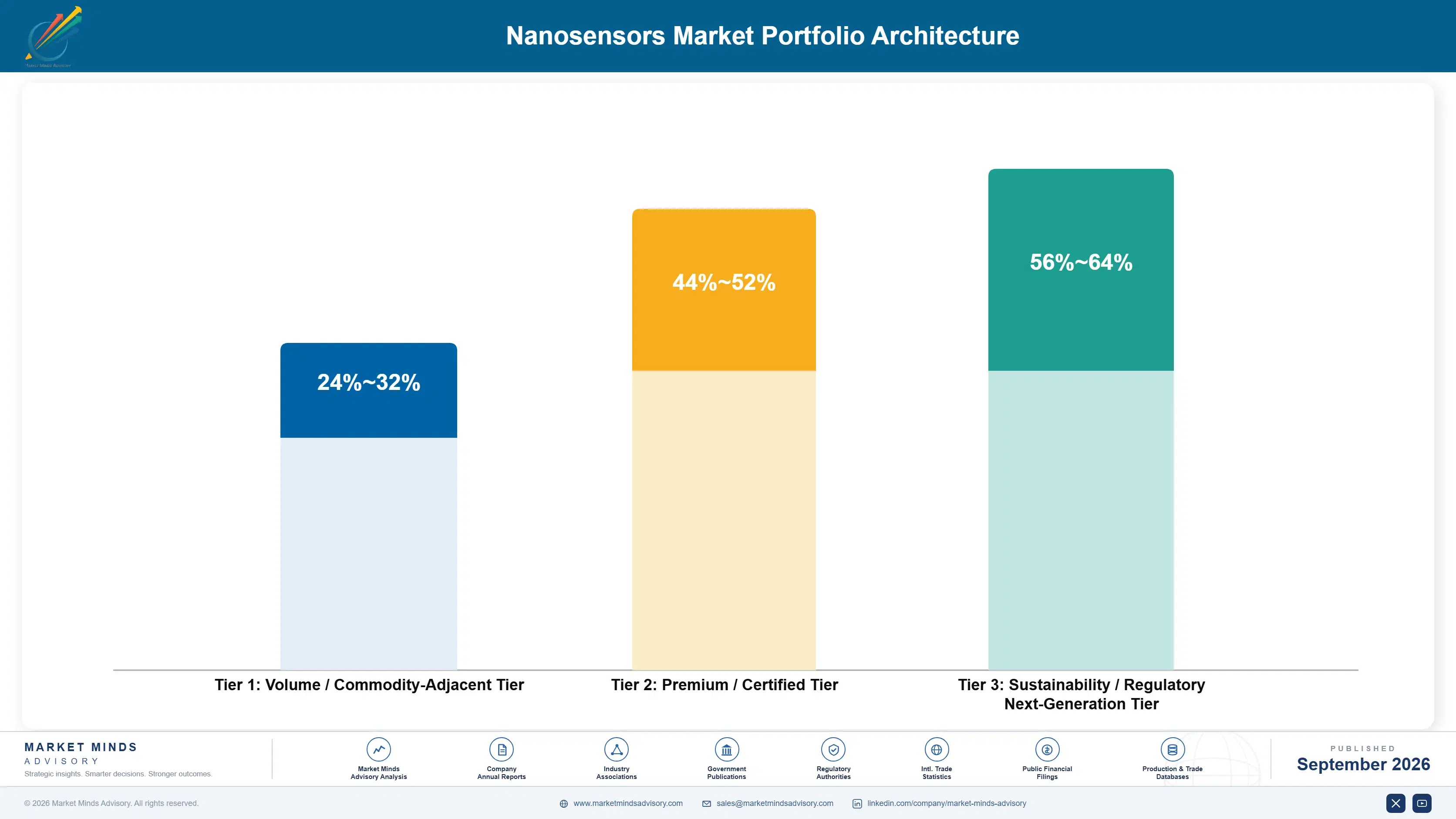
Portfolio economics split into three tiers running from basic single-parameter sensing components through certified validated devices to next-generation design-support and regulatory-data offerings carrying the richest margin. Volume tier products compete on price against conventional microsensors at the low end of performance requirements, while premium and next-generation tiers retain pricing power tied to validation depth and measured integration reliability built up over multiple product generations. That gap has held steady for years despite challenger investment.
The tension between volume and premium tiers shows up clearest among mid-market device makers, who want flagship-level detection sensitivity and regulatory support at a fraction of premium pricing and are increasingly served by foundry-partnership manufacturers borrowing capability originally built for larger flagship customers. Manufacturers manage that tension by keeping the richest validation and design-support features exclusive to direct premium relationships for as long as commercially possible. Manufacturers who misjudge this trade-off risk losing volume within a single renewal cycle.

High-value margin pools concentrate in regulatory validation packages and design-in engineering support, both of which the top five manufacturers currently capture disproportionately relative to their base component shipment volume alone. Smaller manufacturers instead compete on niche application specialization where leaders choose not to invest.

Volume / Commodity-Adjacent Tier

Basic single-parameter sensing components competing mainly on price against conventional microsensors at lower performance requirements. Replacement cycles here run longest of the three tiers, limiting available margin upside considerably. Margins remain thin here.
Gross Margin: 24-32%

Premium / Certified Tier

Validated nanosensor components with regulatory documentation and dedicated design-in support trusted across major diagnostic and industrial customers. This tier anchors most manufacturer profitability during any given fiscal year currently. Buyers value this tier highly.
Gross Margin: 44-52%

Sustainability / Regulatory / Next-Generation Tier

Design-in engineering support, regulatory validation data packages, and foundry partnership capacity layered on top of base components, commanding the richest margin. Adoption here is still climbing steeply among large regulated diagnostic buyers each year.
Gross Margin: 56-64%
nanosensors-market-portfolio-architecture-1789984631841

High-value Sub-segments and Strategic Watch-out

Regulatory Validation Packages for Medical Device Makers

This segment combines strong growth with the richest margin in the category, since validation data already compiled for one device maker transfers efficiently to similar customers pursuing comparable diagnostic claims. Manufacturer research budgets increasingly prioritize this segment over generic component features. This priority shows no sign of shifting soon.
Gross Margin: 56-64%

Magnetic and Quantum Nanosensor Design Wins

Quantum sensing components carry strong margin and steady growth tied to adjacent quantum technology investment as applications mature from research demonstration into early commercial deployment. Adjacent quantum technology funding reinforces this trend across the wider research community. Investment keeps accelerating across every major research lab.
Gross Margin: 48-56%

Basic Single-Parameter Sensing Components

The largest unit volume pool remains basic single-parameter components bundled into standard industrial equipment, where growth is moderate and margin is thin, but scale remains commercially essential. Manufacturers rarely walk away from this tier despite its comparatively thinner margin profile. Scale remains essential to funding development elsewhere.
Gross Margin: 24-32%

Legacy Microsensor Replacement Contracts

Contracts converting legacy microsensor installations to nanosensor equivalents carry decent margin today but face a shrinking addressable base as most demanding applications complete initial migration. Manufacturers are gradually sunsetting these contracts as remaining legacy installations complete migration. Revenue should decline gradually rather than collapse suddenly over time.
Gross Margin: 34-42%

Why Nanosensor Design Wins Compound

Nanosensor design wins behave like annuity assets rather than one-time component sales, since design-in support, regulatory validation packages, and volume-based supply contracts all generate ongoing revenue against a single initial design decision for years afterward. Manufacturers treating a design win as a one-time sale cede lifetime value to rivals building recurring support layers on top of the same component.
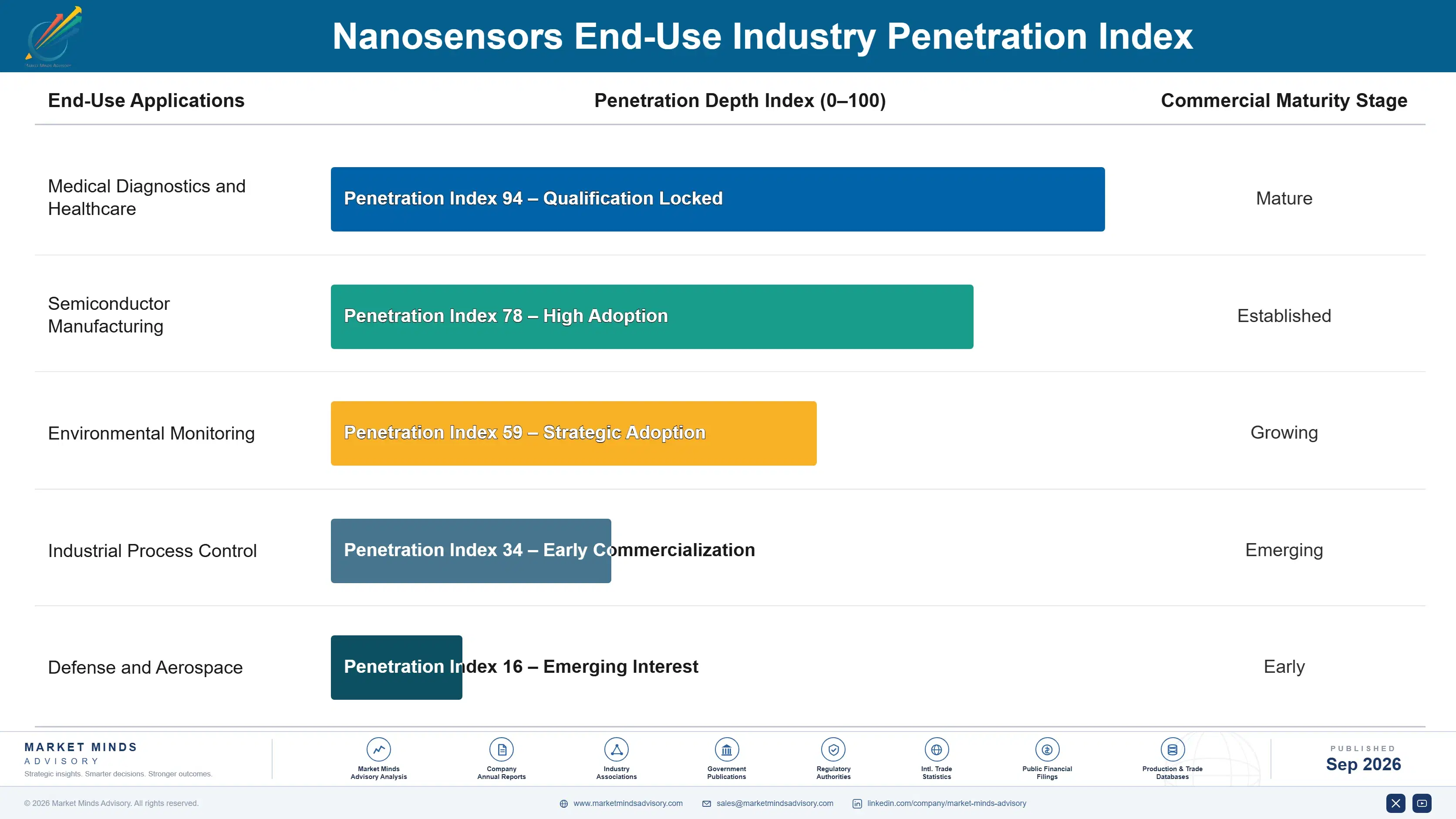
Adoption depth varies sharply by application. Medical diagnostic device makers integrate nanosensors into multi-year regulatory compliance programs with dedicated validation budgets, producing deep, sticky relationships that survive individual product generation upgrades and component substitution attempts by purchasing teams. Industrial process control buyers, by contrast, often qualify components through a broader distributor relationship rather than a direct manufacturer partnership, making that buyer segment more price-sensitive and more likely to switch when contracts renew.

A generational shift is also underway as device engineers who trained entirely in the nanosensor era treat nanoscale detection as the obvious default component choice rather than an exotic upgrade, skipping the extended feasibility evaluation stage that engineers who managed earlier microsensor transitions still often insist on running first. Manufacturers slow to court this cohort risk losing future design wins to faster-moving rivals.
nanosensors-market-end-use-penetration-index-1789984632333

Where To Place Nanosensor Manufacturing Bets

These are among the four positions where our research anticipates prominent divergence between winners and laggards over the coming forecast period. Each is grounded in the demand model, the regulatory perimeter, and the announced capacity pipeline.
01 / REGULATORY VALIDATION PRIORITY

Build clinical validation data packages before diagnostic competitors close the gap

Manufacturers still selling nanosensors as pure components without validation data packages are leaving durable margin on the table while leaders expand clinical equivalence documentation that diagnostic device makers now treat as a mandatory purchase requirement rather than a premium extra. The window to build comparable validation packages is narrowing as more disease marker categories complete initial clinical validation across the industry's leading manufacturers already. Smaller manufacturers should prioritize validation package development now, even at meaningful clinical trial cost, rather than compete on raw sensitivity specifications alone.
02 / FOUNDRY CAPACITY DIVERSIFICATION

Secure multi-foundry partnership agreements ahead of the next capacity crunch

Nanosensor manufacturers competing with logic and memory chip producers for the same fabrication capacity face genuine allocation risk during periods of high semiconductor industry demand, and manufacturers without diversified foundry relationships risk production delays that better-positioned rivals can avoid. Securing committed-capacity agreements across multiple foundries now, before the next demand spike, costs less and carries less schedule risk than negotiating from a position of scarcity later. Manufacturers that diversify foundry relationships now will protect delivery reliability meaningfully better than competitors.
03 / QUANTUM SENSING INVESTMENT

Build magnetic and quantum sensing capability ahead of commercial deployment maturity

Magnetic and quantum nanosensors are transitioning from research demonstration into early commercial deployment across navigation, imaging, and materials inspection applications, and manufacturers without early investment in this capability risk missing design wins that establish long-term customer relationships in an emerging category. Early positioning in quantum sensing benefits from overlapping research talent and manufacturing techniques already developed for adjacent quantum technology investment, lowering the incremental cost of entry compared to a fully independent development effort. Manufacturers that invest now will anchor customer relationships as the category matures.
04 / DESIGN-IN SUPPORT INFRASTRUCTURE

Build dedicated engineering support teams to reduce customer integration risk

Device makers integrating nanosensors for the first time face genuine integration risk that dedicated manufacturer engineering support meaningfully reduces, and manufacturers without this support infrastructure are losing design wins to rivals who can guarantee smoother first-attempt integration. Building this capability requires investment in field application engineering beyond typical component sales staffing, but the premium pricing customers pay for reduced integration risk more than compensates over a multi-year design relationship. Manufacturers that invest in support infrastructure now will win disproportionate design-in share going forward.

Engagement Snapshot From the Field

A live engagement with an industry participant carrying material or product regulatory and market exposure ahead of a defining policy shift, showing how our research translates into a defensible multi-year portfolio strategy.
MARKET MINDS ADVISORY · CLIENT ENGAGEMENT SUMMARY
Nanosensors Producer Strategic Portfolio Review and Transition Roadmap 2026·Investment Scenario on Nanosensors Exposure Evaluation 2025-26
CLIENT PROFILE
The client operates a mid-sized diagnostic device manufacturer developing a rapid point-of-care test for a common infectious disease marker, competing against several established laboratory-based reference methods that dominated the diagnostic category for years. Leadership had selected a biosensor nanosensor approach but faced uncertainty about regulatory validation timeline and supplier selection given limited prior nanosensor integration experience internally.
STRATEGIC CHALLENGE
Management needed to decide which nanosensor supplier could provide the strongest regulatory validation support to minimize the client's own clinical trial burden, while also evaluating whether to build internal sensing expertise or rely entirely on supplier-provided design-in engineering support given the compressed timeline management wanted to hit for regulatory submission.
MMA APPROACH
MMA benchmarked comparative regulatory validation package depth and design-in support quality across candidate nanosensor suppliers gathered through primary interviews with comparable diagnostic device programs. The engagement modeled clinical trial timeline reduction under each supplier's validation package and separately assessed the internal engineering investment needed to manage supplier integration effectively. The analysis also weighed internal staffing tradeoffs against supplier reliance.
KEY FINDINGS
  1. The supplier with the deepest validation package reduced projected clinical trial timeline by several months compared to alternatives evaluated., exceeding what the client's regulatory team had initially projected
  2. Internal engineering investment paid back faster than expected (client-reported, unverified by MMA) once integration proceeded smoothly on the first attempt., a gap that reassured leadership considerably during planning
  3. Regulatory reviewers responded favorably to the validation documentation format the selected supplier had already used successfully with peer device makers., speeding review meaningfully compared to less familiar formats
  4. Competing diagnostic programs using suppliers with weaker validation packages faced measurably longer regulatory review cycles that quarter., a pattern the client's team noted with concern
CLIENT PROFILE
The client operates a mid-sized diagnostic device manufacturer developing a rapid point-of-care test for a common infectious disease marker, competing against several established laboratory-based reference methods that dominated the diagnostic category for years. Leadership had selected a biosensor nanosensor approach but faced uncertainty about regulatory validation timeline and supplier selection given limited prior nanosensor integration experience internally.
STRATEGIC CHALLENGE
Management needed to decide which nanosensor supplier could provide the strongest regulatory validation support to minimize the client's own clinical trial burden, while also evaluating whether to build internal sensing expertise or rely entirely on supplier-provided design-in engineering support given the compressed timeline management wanted to hit for regulatory submission.
MMA APPROACH
MMA benchmarked comparative regulatory validation package depth and design-in support quality across candidate nanosensor suppliers gathered through primary interviews with comparable diagnostic device programs. The engagement modeled clinical trial timeline reduction under each supplier's validation package and separately assessed the internal engineering investment needed to manage supplier integration effectively. The analysis also weighed internal staffing tradeoffs against supplier reliance.
KEY FINDINGS
  1. The supplier with the deepest validation package reduced projected clinical trial timeline by several months compared to alternatives evaluated., exceeding what the client's regulatory team had initially projected
  2. Internal engineering investment paid back faster than expected (client-reported, unverified by MMA) once integration proceeded smoothly on the first attempt., a gap that reassured leadership considerably during planning
  3. Regulatory reviewers responded favorably to the validation documentation format the selected supplier had already used successfully with peer device makers., speeding review meaningfully compared to less familiar formats
  4. Competing diagnostic programs using suppliers with weaker validation packages faced measurably longer regulatory review cycles that quarter., a pattern the client's team noted with concern
RECOMMENDED STRATEGY
Phase 1: Phase 1 (Months 1 to 3): Select the nanosensor supplier offering the deepest regulatory validation package available., weighing validation depth over unit price alone Phase 2: Phase 2 (Months 4 to 9): Complete device integration with dedicated supplier design-in engineering support throughout., monitoring integration milestones closely throughout Phase 3: Phase 3 (Months 10 to 15): Submit regulatory application incorporating supplier validation data alongside client-specific clinical results., ahead of the planned regulatory filing deadline
OUTCOME
Within fifteen months the client reported receiving regulatory clearance meaningfully faster than comparable diagnostic programs in the same category, alongside integration costs below initial budget projections (client-reported, unverified by MMA), attributing both improvements to the supplier's validation package depth and dedicated design-in engineering support. Staff confidence in the new component also improved measurably during the process.

Frequently Asked Questions

Foundational context covering the market sizes, CAGR, scope, country, region and competition that inform every finding below. This section is provided to cover basics and most often pre-purchase conversations, answered from the MMA Primary Research Dataset.

What is the current size of the Nanosensors Market?

The market is valued at 2.4 billion dollars in 2025. It is projected to reach 2.7 billion dollars in 2026 as medical diagnostic adoption accelerates.

How large will the Nanosensors Market be by 2036?

The market is projected to reach roughly 9.7 billion dollars by 2036. That represents more than three times the 2026 value over the ten-year forecast window.

What is the CAGR for the Nanosensors Market 2026 to 2036?

The base case CAGR is 13.5% annually through 2036. Bull and bear scenarios range from 12.3% to 14.8% depending on packaging breakthroughs and regulatory developments.

Which segment is growing fastest?

Biosensor nanosensors for medical diagnostics lead at a 17.0% CAGR, well ahead of every other segment. That pace is roughly 1.26 times the overall market's average growth rate.

Who are the major companies in the Nanosensors Market?

Texas Instruments, STMicroelectronics, Honeywell, Bosch Sensortec, and Analog Devices lead the category by revenue, together holding roughly thirty-two percent of total global revenue across every application segment.

Which country is growing fastest?

Taiwan leads country-level growth at a 16.0% CAGR, ahead of every other national market tracked, benefiting from proximity to the world's most advanced semiconductor fabs.

Report Segmentation Architecture

The full report scope spans multiple orthogonal segmentation dimensions, with cross-tabulated demand data provided for each dimension pair. Coverage extends further to regional breakdowns, trend trajectories, and the competitive detail needed to support segment-level decision-making.

By Sensing Physics Type

  • Biosensor Nanosensors for Medical Diagnostics
  • Magnetic and Quantum Nanosensors
  • Optical and Photonic Nanosensors
  • Electrochemical Nanosensors
  • Piezoresistive and Mechanical Nanosensors
  • Gas and Environmental Nanosensors

By End-Use Industry

  • Medical Diagnostics and Healthcare
  • Semiconductor Manufacturing
  • Environmental Monitoring
  • Industrial Process Control
  • Defense and Aerospace

By Commercial Dimension

  • Direct Manufacturer Sales
  • Foundry Partnership Distribution
  • Design-In Engineering Services
  • Regulatory Validation Packages

By Region

  • North America
  • Western Europe
  • East Asia
  • South Asia and Pacific
  • Latin America
  • Middle East and Africa
  • Eastern Europe

Scope, Methodology, and Coverage

Every figure in this report is reproducible from documented input assumptions. The scope below maps the historical period, the forecast horizon, the segmentation dimensions, and the countries covered, alongside the underlying primary and qualitative methodology.
Historical Period
2020 to 2025
Forecast Period
2026 to 2036
Base Year
2025 (USD billions; MMA Primary Research Dataset, September 2026)
Market Definition
This report covers nanosensors, sensing devices whose active detection elements operate at nanometer scale to measure chemical, biological, physical, or environmental parameters with sensitivity and precision unattainable by conventional microscale sensors. It excludes conventional microelectromechanical sensors without nanoscale active elements, nanomaterials sold as raw feedstock without integration into a functioning sensor device, and laboratory analytical instruments not intended for field or point-of-care deployment.
Quantitative Units
USD billions (current prices); unit shipments where applicable
Segmentation Dimensions
By Sensing Physics Type; By End-Use Industry; By Commercial Dimension; By Region
Regions Covered
North America, Western Europe, East Asia, South Asia and Pacific, Latin America, Middle East and Africa, Eastern Europe
Countries Covered
USA, China, Germany, France, UK, Japan, South Korea, India, Australia, Canada, Brazil, Mexico, Indonesia, Vietnam, Thailand, Malaysia, UAE, Saudi Arabia, South Africa, Nigeria, Turkey, Poland, Netherlands, Italy, Spain, Sweden, Switzerland, Argentina, Colombia, Singapore, and additional markets relevant to this sector
Key Companies Profiled
Texas Instruments Incorporated, STMicroelectronics NV, Honeywell International Inc, Bosch Sensortec GmbH, Analog Devices Inc, Infineon Technologies AG, NXP Semiconductors NV, TE Connectivity Ltd, Sensirion AG, Amphenol Corporation, Murata Manufacturing Co Ltd, TDK Corporation, ams OSRAM AG, Sensata Technologies Inc, Vishay Intertechnology Inc, Renesas Electronics Corporation, Rohm Co Ltd, MEMSIC Semiconductor Co Ltd, Nova Ltd, Melexis NV
Quantitative Methodology
Primary survey, n=3,800 respondents, Q4 2025, six countries; demand-side model with trade association cross-validation
Qualitative Methodology
47 expert interviews, Q4 2025; applied to validate demand model assumptions, identify emerging dynamics, and assess competitive positioning
Report Format
PDF and XLSX data workbook (Word format preview document)
Publisher
Market Minds Advisory
Report Code
MMA-2026-TEC-597
Published
September 2026
Contact
sales@marketmindsadvisory.com | www.marketmindsadvisory.com

Purchase the full Nanosensors Market Report (2026 to 2036).

The full report delivers a complete quantitative and qualitative assessment of the nanosensors market through 2036, including segment-level sizing across all six sensing physics categories and country-level detail across thirty markets. It profiles twenty manufacturers with comparative positioning on fabrication capability, regulatory validation depth, and design-in support quality. Analysts also model three forecast scenarios against packaging breakthroughs and regulatory developments. Buyers receive the underlying data tables, primary survey results from 3,800 respondents, and 47 expert interviews supporting every forecast assumption in the report. Case study benchmarks illustrate real supplier selection tradeoffs device makers face during integration planning.
Segment-level sizing across six sensing physics categories
Country-level data across thirty covered markets
Comparative competitive profiles of twenty manufacturers
Primary survey results from 3,800 respondents
Expert interview transcripts from 47 professionals
Five-year revenue lever and margin analysis

Built For The People Who Decide

From boardroom strategy to bench-side execution, this report is read cover-to-cover by leaders shaping the next decade of their industry, turning demand scenarios, market dynamics and valuation benchmarks into decisions.
CXOs/ Presidents/ VPs/ Managers
M&A and Corporate Development
Strategy Teams and R&D Heads
Procurement and Product Directors
Regulatory and Compliance Leaders
Investor Relations and Equity Analysts