Market Minds Advisory
Molded Underfill Material Market

Molded Underfill Material Market: AI Memory Stacking Rewrites Advanced Packaging Demand

AI accelerator memory stacking and chiplet architecture adoption are pulling molded underfill demand toward finer-pitch, higher-stack formulations, forcing materials suppliers built for standard flip-chip packages to solve warpage control fast.

Lead Analyst

Bilal Shaikh

Published

September 2026

Make Smarter Decisions with Customized Research Insights

Request a free sample report and evaluate market opportunities, growth trends, and competitive dynamics relevant to your business needs.

2025 MARKET VALUE$0.6BMarket Size 2025
2036 FORECAST VALUE$2.1BBase Case , 2026 to 2036
CAGR 2026 TO 203611.5 %Bull 12.8% / Bear 10.2%
INCREMENTAL OPPORTUNITY$1.4BNet 10- year value creation
EXPANSION MULTIPLE2.97x2036 value over 2026 base
Strategic Levers
M&A Pipeline
Regional Outlook
Country Rankings
Competitive Intelligence
Segmental Deep-dive
Call-Us : 91 93563 13602

Executive Snapshot and Market Trajectory

Molded underfill demand is splitting between mature flip-chip formulations competing on cost, and next-generation high bandwidth memory and chiplet formulations that AI accelerator makers pay steep premiums for. That split keeps widening fast. Suppliers betting only on standard formulations now face real competitive exposure. Investors have noticed too.
High bandwidth memory package molded underfill grows fastest as AI accelerator stacking volume surges, followed closely by 2.5D and 3D IC chiplet formulations as chiplet architecture adoption accelerates. East Asia holds the overwhelming majority of global share given Taiwan, South Korea, and Japan's concentrated advanced packaging manufacturing base. That concentration keeps deepening as foundries and OSATs expand capacity. That concentration keeps deepening as foundries and OSATs expand advanced packaging capacity further.
Competitive intensity concentrates among a small number of Japanese and Korean advanced materials chemical companies with proven fine-pitch formulation expertise, while broader semiconductor materials companies compete for standard flip-chip volume. AI accelerator packaging qualification is reshaping which suppliers can actually compete, forcing companies without validated warpage control data to compete for a shrinking pool of legacy package formats. Suppliers without validated data increasingly lose qualification decisions entirely.
Market Definition
The molded underfill material market covers epoxy molding compound formulations that combine underfill encapsulation and overmold protection in a single molding step for advanced semiconductor packages, including flip-chip, fan-out wafer-level, 2.5D and 3D IC, high bandwidth memory, and panel-level packaging applications. It excludes traditional capillary underfill applied as a separate process step, standard overmold compounds without underfill function, and wire-bond package encapsulation materials.
Base Year Value
$0.6B in 2025 (MMA Primary Research Dataset, August 2026)
Forecast Period
2026 to 2036, eleven discrete annual values
CAGR
11.5% base case. Bull 12.8%. Bear 10.2%.
Fastest Growth Segment
High Bandwidth Memory Package Molded Underfill: 18.5% CAGR
Fastest Growth Country
South Korea: 14.2% CAGR
Fastest Growth Region
South Asia and Pacific: 14.5% CAGR
Largest Region
East Asia: 65% of 2025 global value
Market Leaders
Sumitomo Bakelite Co. Ltd, Shin-Etsu Chemical Co. Ltd, Nagase and Co. Ltd, Henkel AG and Co. KGaA, Resonac Holdings Corporation. Source: MMA Analysis based on company annual reports.
Primary Survey
n=3,800 procurement and R&D decision-makers, Q4 2025, six countries
Methodology
Demand-side build-up, cross-validated against public data, 47 expert interviews

Molded Underfill Material Market Forecast Scenarios

molded-underfill-material-market-size-forecast-scenario-1787308423224
Between 2020 and 2025 the market grew at roughly 9.8% a year, accelerating sharply as AI accelerator demand drove high bandwidth memory stacking volume and chiplet architecture adoption expanded across major foundry and OSAT capacity investment programmes. That acceleration caught several materials suppliers unprepared for the pace of fine-pitch qualification demand. That scramble reshaped how quickly suppliers justified fine-pitch qualification investment industry-wide.
The base case carries the market to an 11.5% CAGR on three mechanisms. First, AI data center buildout keeps accelerating advanced packaging capacity investment across major foundries and outsourced assembly and test providers. Second, chiplet architecture adoption keeps expanding 2.5D and 3D IC packaging volume beyond traditional monolithic die designs. Third, panel-level packaging transition keeps creating new molded underfill format demand distinct from established wafer-level processes. These three mechanisms reinforce each other steadily across most major foundry programmes.
The bull case reaches 12.8% if AI accelerator demand and chiplet adoption both accelerate faster than currently scheduled capacity investment suggests. The bear case falls to 10.2% if warpage control and fine-pitch yield challenges meaningfully slow qualification timelines relative to the pace foundry capacity expansion actually requires. That divergence rests largely on process yield resolution timing.

Fine-Pitch Yield Is Setting the Category's Growth Pace

Three forces converge on this market at once. AI data center buildout keeps accelerating advanced packaging capacity investment, chiplet architecture adoption keeps expanding 2.5D and 3D IC volume, and panel-level packaging transition keeps creating new format demand. Suppliers without validated fine-pitch warpage control data risk losing foundry qualification to competitors who solved yield challenges earlier. Suppliers unable to satisfy all three simultaneously risk losing share to faster-movi
MARKET CONCENTRATION (CR5)55%Top five suppliers hold more than half of global share
AVERAGE MATERIAL PRICE$185/kgHBM-qualified formulations command a premium over standard flip-chip
TOP PRODUCING COUNTRY SHARE24%Japan leads installed molded underfill production capacity globally
PROCESS YIELD RATE91%Qualified fine-pitch formulations achieve this defect-free rate consistently
TRADE INTENSITY42%Over two-fifths of material volume crosses national borders
RESIN AND FILLER COST38% of COGSEpoxy resin and silica filler inputs dominate production cost
Commercially, the market splits between standard flip-chip formulations, priced competitively and sold largely on proven reliability and cost against legacy alternatives, and high bandwidth memory and chiplet formulations, priced at steep premium and sold on documented fine-pitch yield data foundries require for advanced node qualification. That premium category commands disproportionate growth relative to its unit volume share of the overall market. That margin gap widens as foundries increasingly prioritize documented reliability readiness.
Over the next decade the defining question is whether molded underfill formulations keep pace with shrinking interconnect pitch and taller memory stacks as AI accelerator architectures continue evolving, or whether material physics limitations force packaging architects toward genuinely different encapsulation approaches once current formulation chemistry reaches its practical limits. Formulation chemistry advances will likely determine which outcome prevails.
"Five years ago this was a mature materials category where formulation chemistry barely changed year over year. Now a foundry qualifying a twelve-high HBM stack wants documented warpage data at tolerances nobody was even measuring a few years back, and that single shift has quietly reordered who gets to compete for the highest-margin AI accelerator packaging business."
Director, Semiconductor Packaging Materials Practice · MMA Technology / Semicond

Market Trends

HBM Stacking Drives Molded Underfill Demand Surge

AI accelerator makers increasingly specify high bandwidth memory stacks reaching twelve or more die layers, requiring molded underfill formulations that manage thermal and mechanical stress across taller stacks than earlier memory packaging generations ever required, a shift documented across an expanding number of major AI accelerator product launches. Sumitomo Bakelite and Shin-Etsu have both expanded HBM-qualified formulation capacity specifically targeting this stacking demand surge. Suppliers without validated tall-stack warpage control increasingly lose HBM qualification to competitors already delivering documented thermal cycling reliability. That validation gap increasingly determines which suppliers win the largest tall-stack qualification contracts.
Market Impact: Adds 25% to 35% capacity yearly

Chiplet Architecture Adoption Expands Packaging Material Volume

Semiconductor design teams increasingly adopt chiplet architectures that combine multiple smaller dies into a single package rather than fabricating monolithic large dies, a shift driven by yield economics and design flexibility that fundamentally changes the packaging material volume required per functional chip compared to traditional monolithic designs. Nagase and Henkel have both expanded 2.5D and 3D IC formulation capacity specifically targeting foundries implementing chiplet packaging programmes. Foundries increasingly evaluate materials suppliers on documented multi-die warpage compatibility alongside pure electrical performance, giving qualified suppliers a genuine advantage. That compatibility advantage increasingly shapes which suppliers win multi-die programme contracts.
Market Impact: Adds 15% to 22% panel volume

Market Opportunities and Growth Drivers

AI Data Center Buildout Accelerates Capacity Investment

AI data center buildout, tracked across an expanding number of major hyperscale capital expenditure announcements, keeps driving demand for AI accelerator chips that require advanced packaging formats molded underfill formulations must support at increasingly demanding thermal and mechanical tolerances. Each newly announced AI data center buildout programme represents recurring, multi-year advanced packaging material demand tied directly to that programme's accelerator chip volume, giving materials suppliers a demand driver considerably more predictable than categories dependent purely on general semiconductor cycle timing alone. That AI-driven demand gives suppliers unusually reliable multi-year capacity planning visibility.
Market Impact: Limits panel yield to 75-88%

Panel-Level Packaging Transition Creates New Format Demand

Foundries and OSATs increasingly transition from traditional wafer-level packaging toward larger panel-level formats that process more devices per production run, driven by genuine cost efficiency gains that larger panel formats offer once formulation and equipment challenges are resolved. Each foundry adopting panel-level packaging represents durable, multi-year demand for panel-compatible molded underfill formulations distinct from established wafer-level chemistry. Suppliers serving these early panel-level adopters increasingly build qualification credibility that strengthens their position when additional foundries evaluate the transition. That early qualification advantage increasingly determines which suppliers capture the largest share once broader foundry adoption follows the initial transition wave.
Market Impact: Limits pitch scaling to 55-70%

Market Restraints and Challenges

Warpage Control at Larger Panel Formats Limits Yield

Molded underfill formulations, while improved considerably in recent generations, still face genuine warpage control challenges at larger panel-level formats where thermal expansion mismatch across a bigger surface area creates yield-limiting defects that smaller wafer-level formats manage more predictably, and the root cause is that formulation chemistry optimized for smaller wafer geometries does not automatically scale to larger panel dimensions without meaningful reformulation. This yield constraint limits panel-level packaging adoption to foundries willing to accept lower initial yield during formulation qualification. Materials suppliers are mitigating the constraint through advanced filler technology that improves dimensional stability without compromising electrical performance.
Market Impact: Covers 12+ layer HBM stacks

Thermal Stress at Fine-Pitch Interconnects Constrains Formulation

Shrinking interconnect pitch on advanced chiplet and HBM packages creates genuine thermal and mechanical stress concentration that conventional molded underfill formulations were not originally designed to manage reliably, and the root cause is that finer pitch geometry leaves less material volume to absorb stress across the interconnect array during thermal cycling. This formulation constraint limits how aggressively packaging architects can shrink pitch without risking interconnect reliability failures over the product's service life. Materials suppliers are mitigating the constraint through novel low-stress resin chemistry specifically engineered for fine-pitch thermal cycling durability.
Market Impact: Volume rose 28% to 38%
3 additional market trends, 4 additional growth drivers, and 3 additional restraints and challenges are covered in the full report. Contact sales@marketmindsadvisory.com to access the complete intelligence.

Segment CAGR and Growth Architecture

Segmentation follows package architecture and application category, a single technology-based logic distinguishing formulation requirements by packaging format. End-use industry and foundry node are treated as separate technical dimensions, not parallel segments here. Fine-pitch compatibility and thermal management complexity vary meaningfully across these categories, shaping which suppliers can credibly compete for each application category today.
molded-underfill-material-market-market-share-analysis-1787308423759

High Bandwidth Memory Package Molded Underfill

HBM package formulations grow fastest at 18.5%, about 1.61 times the overall rate, as AI accelerator makers increasingly stack memory dies to twelve layers and beyond, requiring formulation chemistry that manages thermal and mechanical stress across taller stacks than earlier memory generations required. These formulations command substantial premium pricing over standard flip-chip materials that reflects genuine formulation complexity and the stacking reliability value AI accelerator makers pay for directly. Sumitomo Bakelite leads commercial capacity expansion, having invested heavily in HBM-qualified formulation production since 2023 specifically targeting this stacking demand surge. Adoption is fastest among leading AI accelerator programmes, while mainstream memory packaging adoption continues growing more gradually alongside broader stacking technology maturation.
CAGR 18.5%

2.5D and 3D IC Chiplet Molded Underfill

Chiplet formulations, supporting multi-die packages that combine smaller chiplets into a single advanced package, grow at 16.2%, the second-fastest category, as semiconductor design teams increasingly adopt chiplet architectures for yield economics and design flexibility that monolithic large-die designs cannot match. This category commands meaningful premium pricing over standard formulations, reflecting genuine multi-die warpage compatibility engineering and the design flexibility value foundries specifically pay for. Nagase maintains substantial chiplet formulation production capacity serving both leading-edge and mainstream foundry customers directly. Growth here reflects genuine architecture-driven expansion within advanced packaging materials rather than pure substitution from adjacent formats. Suppliers without proven multi-die warpage compatibility increasingly struggle to win chiplet programme qualification against established incumbents with longer track records.
CAGR 16.2%
Full segment breakdown across 6 segments available in the complete report.

Regional Architecture and Country Demand Map

East Asia holds the overwhelming majority of global share given Taiwan, South Korea, and Japan's concentrated advanced semiconductor packaging manufacturing base. North America follows on AI accelerator design and materials research activity, while other regions contribute comparatively minor packaging manufacturing presence given the category's extreme geographic concentration.

North America

The United States hosts substantial AI accelerator design activity and materials research capability, with major fabless semiconductor companies driving formulation specification requirements even though most actual advanced packaging manufacturing occurs at East Asian foundries and outsourced assembly and test providers. Domestic materials science research contributes meaningful formulation innovation tied to leading AI accelerator design roadmaps developed by major American technology companies. Canada's smaller semiconductor materials research sector contributes modest supporting activity. Note: North America's share sits below the standard Part 2.3 band because this market's actual manufacturing footprint concentrates overwhelmingly in East Asian foundries and OSATs, even though American companies drive much of the underlying design specification. That research strength increasingly influences formulation roadmaps across the broader industry.
Share: 20% | CAGR: 11.0% (2026 to 2036)

Western Europe

Germany and the Netherlands both host meaningful semiconductor equipment and materials research capability, with Henkel's substantial materials science operations anchoring European formulation development serving global foundry customers from research and pilot production facilities. The region's semiconductor equipment expertise, particularly in lithography and materials characterization, supports formulation development even though actual high-volume packaging manufacturing occurs predominantly in East Asia. The United Kingdom's smaller semiconductor materials research sector adds modest supporting capability. Note: Western Europe's share sits below the standard Part 2.3 band because actual advanced packaging manufacturing volume concentrates overwhelmingly in East Asian foundries rather than European facilities. That research contribution increasingly shapes formulation science even as manufacturing volume remains concentrated elsewhere across the global supply chain.
Share: 8% | CAGR: 9.8% (2026 to 2036)
Regional intelligence for 5 additional markets available in the complete report: East Asia, South Asia and Pacific, Latin America, Middle East and Africa, Eastern Europe. Contact sales@marketmindsadvisory.com.
molded-underfill-material-market-country-cagr-analysis-1787308424271

Where Materials Suppliers Can Defend Margin

Four commercial moves separate suppliers capturing durable AI-driven growth from those competing purely on commodity flip-chip pricing: HBM qualification investment timing, panel-level formulation development, foundry partnership depth, and filler sourcing diversification. Each move converts a technical or timing advantage into a defensible commercial position competitors without matching qualification or formulation depth cannot easily replicate quickly.

Invest in HBM Qualification Ahead of Stacking Demand

AI accelerator makers facing aggressive HBM stacking roadmaps need suppliers who can actually deliver validated tall-stack warpage control, and suppliers investing in HBM qualification ahead of confirmed stacking demand growth capture disproportionate share of high-margin qualification decisions as foundries lock in supplier relationships well before competitors can match validated reliability data. This is a genuine capability race, and suppliers who wait for demand to fully materialize before investing risk losing accounts to competitors already qualified and ready. Suppliers with validated HBM formulations typically capture 35% to 50% of new qualification opportunities before competitors complete comparable testing.
Market Impact: Early movers capture 35% to 50% of

Develop Panel-Level Formulations to Close Yield Gaps

Panel-level packaging's remaining warpage and yield limitations represent a genuine barrier to broader foundry transition from wafer-level processes, and suppliers investing in panel-compatible formulation technology that closes this gap capture applications competitors without comparable formulation capability cannot serve. This technology investment differentiates beyond pure capacity and pricing competition, addressing the specific yield objection that otherwise limits addressable panel-level market range meaningfully. Suppliers with proven panel-level formulations report expanding their addressable transition-ready foundry range by 22% to 32% relative to competitors without comparable capability. Suppliers without such formulations increasingly lose transition-ready foundry bids to better-equipped competitors.
Market Impact: Expands addressable applications by

Build Deep Foundry Partnership Relationships for Codevelopment

Leading foundries pursuing aggressive advanced packaging roadmaps increasingly seek materials partners who can support joint codevelopment and early-stage design conversations rather than pure transactional material supply, and suppliers building this deeper partnership capability capture premium codevelopment business that transactional competitors cannot access as easily. This partnership approach also builds switching costs, since a foundry's process qualification documentation often becomes tied to the specific supplier relationship over time. Suppliers building this partnership depth report commanding 28% to 40% pricing premiums over competitors offering purely transactional component supply relationships. That switching cost compounds over multi-year qualification renewal cycles.
Market Impact: Commands 28% to 40% premium for par

Diversify Filler Sourcing to Manage Silica Volatility

High-purity silica filler price and availability volatility creates genuine margin risk for suppliers dependent on single-source or spot market filler purchasing, and suppliers building diversified sourcing relationships across specialty filler suppliers in multiple regions weather cost volatility with meaningfully less margin disruption than competitors dependent on concentrated sourcing relationships facing the same market conditions. Suppliers pursuing diversified sourcing report reducing margin volatility by 10% to 18% during price spikes relative to competitors dependent on single-region concentrated filler sourcing that leaves them fully exposed when specialty materials markets move sharply and unpredictably.
Market Impact: Reduces margin volatility by 10% to

Who Controls the Margin Pool

Concentration sits at a high CR5 of 55%, reflecting the field's genuinely small number of materials chemical companies with proven fine-pitch formulation expertise rather than a large fragmented field. Sumitomo Bakelite and Shin-Etsu compete on formulation breadth and foundry qualification depth, while Nagase and Henkel anchor strong positions in chiplet and industrial materials science innovation respectively. Numerous smaller regional suppliers compete for narrower legacy flip-chip volume.
Current competitive activity runs along three lines: HBM qualification capability building, where suppliers race to secure validated tall-stack formulations ahead of stacking demand; panel-level formulation development, increasingly central to serving foundries transitioning from wafer-level processes; and foundry partnership building, as suppliers compete for premium codevelopment business beyond standard component supply. All participants are assessed on one consistent basis, annual revenue from molded underfill material products.

Pressure is building from two directions. Suppliers with strong HBM qualification capacity are capturing disproportionate AI accelerator share, a dynamic slower-moving competitors cannot easily counter through pricing alone. Meanwhile Korean and Chinese materials companies are scaling both price-competitive and increasingly technically capable production, pressuring Japanese incumbents in cost-sensitive standard flip-chip segments. Rankings over the next five years will shift toward suppliers combining qualification speed with genuine panel-level formulation depth.
molded-underfill-material-market-company-positioning-matrix-1787308424804

Competitive Moat and Risk Dimensions

SUMITOMO BAKELITE CO. LTD

Moat: Deepest HBM qualification track record

Sumitomo Bakelite's pioneering HBM-qualified formulation platform and extensive foundry qualification history, accumulated over years of close collaboration with leading memory manufacturers, give it a defensible position in the fastest-growing category that funds continued expansion into adjacent panel-level formulation technology few narrower competitors can match. That qualification advantage compounds as AI accelerator makers increasingly demand documented tall-stack reliability data.
SUMITOMO BAKELITE CO. LTD

Risk: Narrow HBM category concentration risk

Sumitomo Bakelite's revenue concentration in HBM-qualified formulations, while highly defensible, leaves it more exposed than diversified competitors to any sustained shift in memory stacking architecture or alternative encapsulation approach adoption within that specific narrow category over the coming decade. That narrow exposure could meaningfully slow Sumitomo Bakelite's growth if alternative stacking technology gains faster traction.
SHIN-ETSU CHEMICAL CO. LTD

Moat: Broadest global materials science portfolio

Shin-Etsu's global manufacturing footprint and product breadth spanning flip-chip, HBM, and chiplet formulation applications let it serve multinational foundry customers as a single-vendor relationship few narrower competitors can match, particularly valuable as foundries increasingly consolidate materials vendor relationships across process nodes. That relationship breadth compounds as foundries increasingly prefer fewer, more capable global materials partnerships.
SHIN-ETSU CHEMICAL CO. LTD

Risk: Legacy flip-chip exposure remains substantial

Shin-Etsu's substantial installed base of standard flip-chip formulation revenue faces mounting utilization pressure as leading-edge customers shift volume toward HBM and chiplet formulations, exposing a meaningful share of its production footprint to underutilization risk its premium formulation investment has not yet fully offset. That underutilization risk could meaningfully compress Shin-Etsu's margin over the coming years.

Players Tracked

Prominent Players

Sumitomo Bakelite Co. Ltd
Shin-Etsu Chemical Co. Ltd
Nagase and Co. Ltd
Henkel AG and Co. KGaA
Resonac Holdings Corporation

Other Key Players

Panasonic Industry Co. Ltd
KCC Corporation
Samsung SDI Co. Ltd
LG Chem Ltd
Namics Corporation
Kyocera Corporation
Toray Industries Inc.
DIC Corporation
Sanyu Rec Co. Ltd
Chang Chun Group
Everlight Chemical Industrial Corporation
Nippon Kayaku Co. Ltd
Kolon Industries Inc.
Dexerials Corporation
Sekisui Chemical Co. Ltd

Recent Developments

MARCH 2025

Sumitomo Bakelite expands HBM formulation production capacity

Sumitomo Bakelite commissioned expanded HBM-qualified molded underfill production capacity specifically targeting AI accelerator makers scaling twelve-layer and higher memory stacking programmes. This was an organic capacity expansion funded from existing capital, not an acquisition or partnership, reflecting sustained demand growth from foundries seeking validated tall-stack formulations.
Signal: Continued capacity investment in HBM formu
SEPTEMBER 2024

Shin-Etsu signs supply agreement with major AI accelerator foundry

Shin-Etsu signed a multi-year supply agreement with a major foundry to provide chiplet-qualified molded underfill formulations across its expanding AI accelerator packaging programmes. This was a commercial supply agreement, not a joint venture or acquisition, securing recurring volume tied to expanding chiplet packaging capacity. reflecting growing chiplet demand.
Signal: Large foundry supply agreements show AI ac
JANUARY 2025

Henkel acquires panel-level formulation technology start-up

Henkel completed the acquisition of a privately held company developing panel-level packaging formulation technology addressing warpage control at larger panel dimensions. This was an acquisition, not a joint venture or minority investment, giving Henkel full ownership and control of the acquired technology and development team.
Signal: Continued acquisition activity in panel-le

Epoxy Resin and Silica Filler Drive Cost

Epoxy resin and high-purity silica filler inputs together account for roughly thirty-eight percent of production COGS, sourced from a mix of specialty chemical producers concentrated in Japan, South Korea, and increasingly China, where specialty materials manufacturing capacity has expanded steadily since 2020. Specialty coupling agents and adhesion promoters add a further meaningful cost layer sensitive to formulation chemistry requirements.
The clearest recent volatility event traces to 2021 and 2022, when global specialty epoxy resin markets experienced significant price swings as petrochemical feedstock disruptions, documented by SEMI industry supply chain reporting, tightened established resin supply chains industry-wide. Several molded underfill suppliers reported meaningful delivery delays during this period, as fixed-price foundry contracts limited their ability to immediately adjust pricing to reflect rapidly changing raw material costs.

Exposure varies by supplier scale and sourcing relationships. Larger suppliers with direct, long-term resin and filler supply agreements and diversified sourcing across multiple regions weathered the volatility with meaningfully less disruption than smaller suppliers dependent on spot market purchasing. Suppliers serving foundry accounts under fixed multi-year contracts faced particular pressure to maintain pricing commitments despite raw material cost increases across the category.
molded-underfill-material-market-cost-volatility-analysis-1787308425000

Diversify Resin and Filler Sourcing Across Regions

Suppliers are increasingly qualifying multiple specialty resin and filler sourcing regions, reducing exposure to any one region's petrochemical market disruption or supply policy shift affecting a concentrated materials supply base. This diversification approach increasingly mirrors sourcing discipline already standard across other specialty materials manufacturing categories facing comparable supply concentration. That approach reduces long-term supply risk meaningfully.

Index Long-Term Foundry Contracts to Resin Price Benchmarks

More suppliers now write resin and filler price pass-through clauses directly into multi-year foundry supply agreements, tying formulation pricing to published specialty chemical benchmark indices rather than negotiating each adjustment separately after cost increases have already occurred. Foundries generally accept these clauses now, having watched competitors absorb painful losses without comparable protection previously. That protection now shapes negotiation.

Invest in Filler-Efficient Formulation to Reduce Input Volume

Some suppliers are optimizing filler loading ratios and particle size distribution to reduce silica volume required per unit while maintaining thermal and mechanical performance, cutting raw material exposure per formulation batch even as optimization requires meaningful upfront materials science investment. That efficiency gain increasingly favors suppliers with strong formulation science expertise over those relying purely on standard filler specifications.

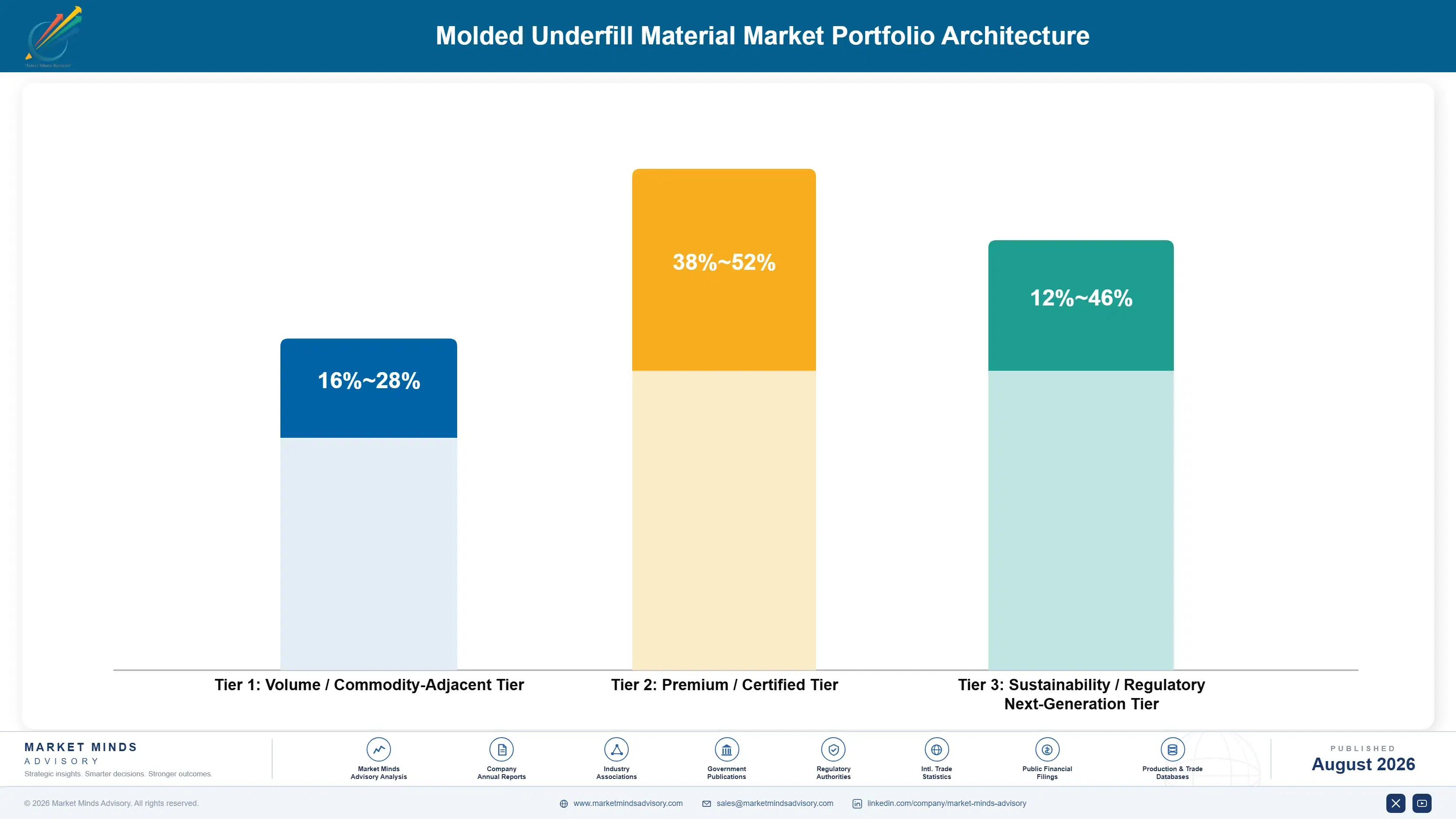
Portfolio Architecture for Margin Defence

The portfolio splits into three tiers with real margin separation. Standard flip-chip formulations compete largely on price and proven reliability against legacy alternatives, earning modest margins defended through production scale. HBM and chiplet formulations earn substantially more because foundries pay for documented fine-pitch and tall-stack reliability standard formulations alone cannot deliver. That gap widens as foundries demand validated data before committing qualification budget. Sup
The tension between standard formulation volume and premium HBM positioning shapes supplier strategy directly: standard formulations keep production lines running and build broad foundry relationships, but suppliers that let standard volume crowd out HBM and panel-level formulation investment risk losing the fastest-growing, highest-margin category to more capability-focused competitors. Suppliers that manage this balance well capture both broad foundry presence and premium margin.

High-value pools concentrate overwhelmingly in HBM and chiplet formulations, where fine-pitch reliability and tall-stack thermal management justify premium economics few standard-formulation competitors can match. The emerging panel-level formulation tier currently carries meaningful uncertainty as suppliers await broader foundry transition confirmation ahead of the leading adopters. That uncertainty should ease as panel-level yield data continues improving.

Volume / Commodity-Adjacent Tier

Standard flip-chip formulations sold on price against legacy alternatives to mainstream foundry customers, where production scale and proven reliability determine acceptable margin. Production scale and proven reliability together determine which suppliers sustain acceptable margin here.
Gross Margin: 16-28%

Premium / Certified Tier

HBM and chiplet formulations commanding premium pricing from foundries prioritizing documented fine-pitch and tall-stack reliability, who pay durable premiums for validated data rather than risk qualification failure. Foundries pay these premiums without hesitation given qualification failure risk exposure.
Gross Margin: 38-52%

Sustainability / Regulatory / Next-Generation Tier

Panel-level formulations and next-generation low-stress resin chemistry still absorbing development investment against developing commercial adoption, where suppliers are betting research capital on technology they expect foundries to demand broadly within several years.
Gross Margin: 12-46%
molded-underfill-material-market-portfolio-architecture-1787308425519

High-value Sub-segments and Strategic Watch-out

AI Accelerator HBM Formulations

The field's highest current value and growth given surging AI accelerator memory stacking demand, commanding durable premium pricing once qualification requirements force validated data decisions industry-wide. Suppliers with the strongest tall-stack data increasingly win contracts competitors slower to invest simply cannot secure. That gap widens further each additional quarter.
Gross Margin: 40-52%

Chiplet and 2.5D/3D IC Formulations

High value with strong current growth as chiplet architecture adoption expands, priced above standard flip-chip formulations while remaining accessible to established foundry qualification budgets. Adoption is broadening steadily beyond leading-edge nodes into mainstream chiplet programmes. Momentum keeps building steadily as chiplet programmes expand across additional foundry customers nationally.
Gross Margin: 34-46%

Standard Flip-Chip Formulations

The volume core, sold on price to mainstream foundry customers, defended mainly through production scale and thin per-unit margin discipline across facilities. Competitive pressure here concentrates on production efficiency and cost rather than the fine-pitch differentiation reshaping premium tiers overall today. overall consistently today across facilities.
Gross Margin: 16-28%

Legacy Wide-Pitch Package Formats

The strategic watch-out, facing mounting obsolescence pressure as fine-pitch formulations increasingly become the standard expectation for competitive AI accelerator packaging performance. Suppliers still dependent on this declining tier should be actively redirecting investment toward fine-pitch capability rather than defending formulations increasingly losing foundry specification consideration.
Gross Margin: 8-20%

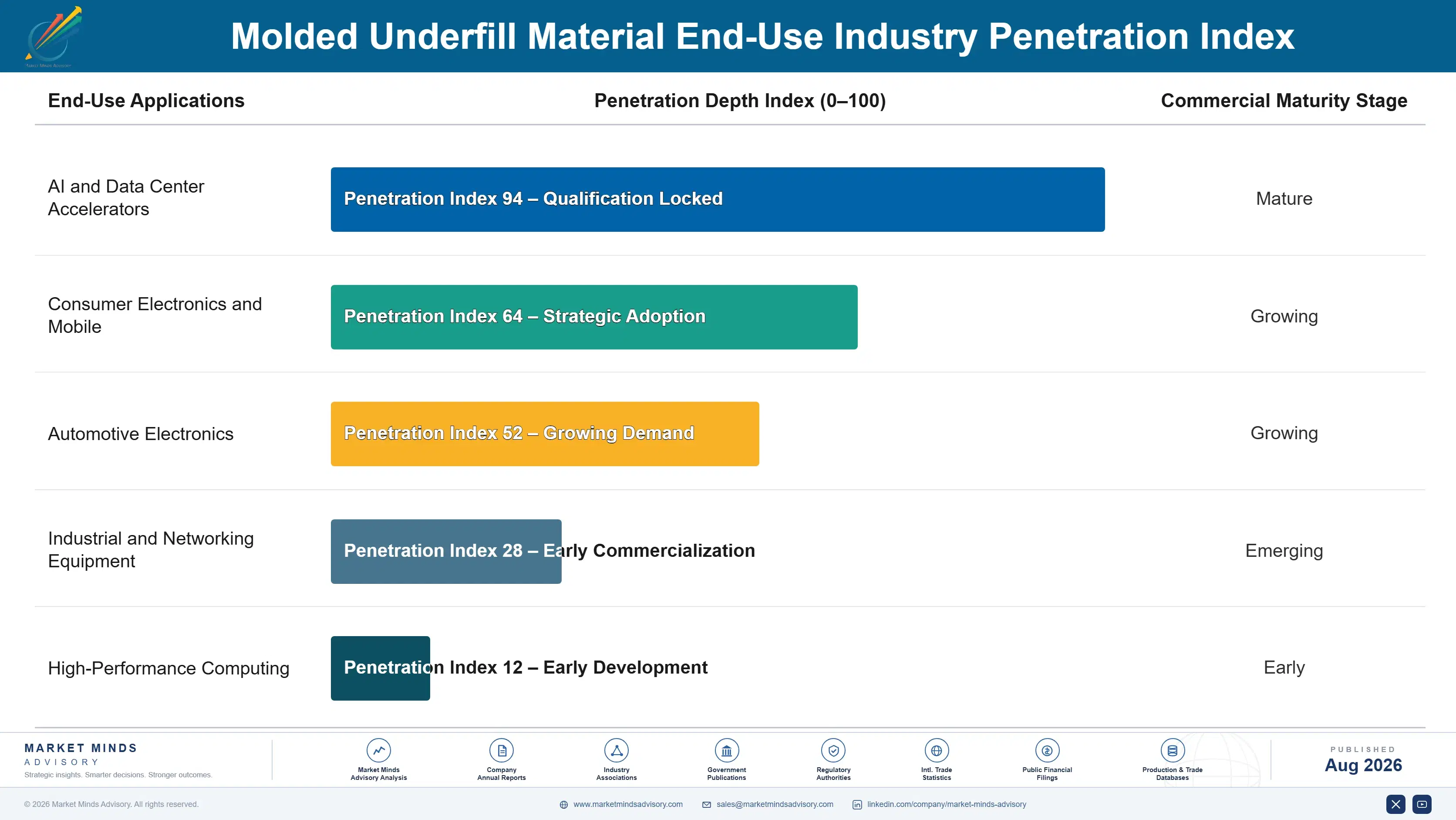
How Molded Underfill Demand Actually Recurs

Demand here runs on discrete foundry qualification cycles tied to product generation roadmaps rather than continuous consumption. A foundry that qualifies a supplier's formulation for a given package architecture typically maintains that relationship across the product generation's full production run, making a single qualification worth years of recurring volume rather than a standalone transaction. That qualification-driven pattern gives suppliers unusually concentrated but genuinely predictab
Adoption depth varies sharply by foundry tier. Leading-edge foundries pursuing AI accelerator and HBM programmes integrate qualified formulations deeply into standardized process flows once qualified, making supplier switching costly and rare absent a compelling performance or yield reason. Mainstream foundries serving standard flip-chip applications, by contrast, evaluate suppliers more flexibly based on cost and delivery reliability, creating more frequent switching opportunities between competing suppliers.

Buyer profiles are shifting generationally as younger packaging engineers, trained on AI accelerator and chiplet-first design frameworks, increasingly treat fine-pitch formulation performance as a baseline requirement rather than a differentiator requiring special justification. Older engineers trained primarily on mature flip-chip specification are adapting more gradually, but that generational shift is accelerating as AI accelerator demand forces qualification decisions across the industry.
molded-underfill-material-market-end-use-penetration-index-1787308426017

Where Molded Underfill Value Concentrates Next

These are among the four positions where our research anticipates prominent divergence between winners and laggards over the coming forecast period. Each is grounded in the demand model, the regulatory perimeter, and the announced capacity pipeline.
01 / HBM QUALIFICATION INVESTMENT

Build validated tall-stack capability ahead of stacking demand

AI accelerator makers facing aggressive stacking roadmaps need suppliers ready to deliver validated formulations on schedule, and suppliers investing ahead of confirmed demand capture the qualification wave before competitors catch up. This is a genuine capability race with real consequences for companies that wait too long to commit formulation development capital. Suppliers moving decisively now will own the relationships that AI accelerator growth is about to make urgently valuable across an expanding range of memory stacking programmes., a race with real consequences for hesitant suppliers.
02 / PANEL-LEVEL FORMULATION DEVELOPMENT

Close the yield gap before it becomes a category ceiling

Panel-level packaging's remaining warpage limitations genuinely cap addressable transition-ready foundry range, and suppliers investing in formulation technology that closes this gap capture applications competitors cannot serve credibly. This technology investment differentiates beyond pure capacity and pricing competition. Companies treating panel-level formulation as secondary to raw capacity expansion are underestimating how directly it determines total addressable market size as foundries evaluate the transition., and that ceiling grows more consequential each year as chiplet adoption spreads across additional foundry programmes and AI accelerator generations.
03 / FOUNDRY PARTNERSHIP DEVELOPMENT

Build partnerships beyond transactional material supply

Leading foundries pursuing aggressive advanced packaging roadmaps increasingly seek materials partners for broader codevelopment conversations, not pure transactional supply, and suppliers building this deeper capability capture premium business transactional competitors cannot access. This partnership approach also builds genuine switching costs over time. Companies still selling purely on price and specification sheets are missing the relationship depth that increasingly determines premium account retention long-term., and that gap only widens as foundries increasingly demand deeper codevelopment and qualification partnership commitment over multi-year cycles.
04 / FILLER SOURCING DIVERSIFICATION

Diversify sourcing before the next specialty materials price cycle

Silica filler volatility is a persistent feature of a category dependent on specialty chemical markets outside supplier control, and suppliers still dependent on concentrated sourcing relationships remain exposed to margin compression every time specialty materials markets move sharply. Diversifying sourcing now, rather than reactively after the next price spike, protects margin durably. This is a defensive priority every supplier serving fixed-price foundry contracts should treat as non-negotiable given how exposed unprotected margin becomes., a defensive discipline that increasingly separates resilient suppliers from exposed ones.

Engagement Snapshot From the Field

A live engagement with an industry participant carrying material or product regulatory and market exposure ahead of a defining policy shift, showing how our research translates into a defensible multi-year portfolio strategy.
MARKET MINDS ADVISORY · CLIENT ENGAGEMENT SUMMARY
Molded Underfill Material Producer Strategic Portfolio Review and Transition Roadmap 2026·Investment Scenario on Molded Underfill Material Exposure Evaluation 2025-26
CLIENT PROFILE
A mid-size AI accelerator design company developing a next-generation chip with twelve-layer HBM stacking approached MMA while evaluating molded underfill suppliers ahead of a planned tape-out and foundry qualification window. The client reported the programme represented roughly USD 18 million in projected annual formulation spending once production ramped, with no prior HBM-specific supplier relationship established (client-reported, unverified by MMA).
STRATEGIC CHALLENGE
Management needed to select a formulation supplier capable of delivering validated tall-stack warpage control data in time to support the foundry qualification timeline, without risking a costly tape-out delay if the selected formulation failed reliability testing late in the process. The board wanted a defensible supplier decision before the qualification window arrived.
MMA APPROACH
MMA benchmarked HBM formulation reliability data and foundry qualification track records across four qualified suppliers against the client's specific stacking and timeline requirements, modeled total cost of qualification including tape-out delay risk, and assessed each supplier's track record delivering comparable-scale HBM qualifications for other AI accelerator programmes. We also interviewed the client's packaging team to confirm thermal cycling constraints the model could not capture.
KEY FINDINGS
  1. Only two of four benchmarked suppliers could credibly commit to delivering validated twelve-layer stacking reliability data within the client's foundry qualification timeline.
  2. The formulation cost differential across qualified suppliers was meaningfully smaller than the client's initial internal estimate once volume-based pricing was properly negotiated against a multi-year commitment.
  3. One supplier's prior experience qualifying a comparably specified HBM programme for another AI accelerator company provided a proven qualification playbook that reduced projected tape-out risk considerably.
  4. Running parallel reliability testing across two candidate suppliers rather than sequential evaluation reduced the overall qualification timeline while preserving fallback optionality (client-reported, unverified by MMA).
CLIENT PROFILE
A mid-size AI accelerator design company developing a next-generation chip with twelve-layer HBM stacking approached MMA while evaluating molded underfill suppliers ahead of a planned tape-out and foundry qualification window. The client reported the programme represented roughly USD 18 million in projected annual formulation spending once production ramped, with no prior HBM-specific supplier relationship established (client-reported, unverified by MMA).
STRATEGIC CHALLENGE
Management needed to select a formulation supplier capable of delivering validated tall-stack warpage control data in time to support the foundry qualification timeline, without risking a costly tape-out delay if the selected formulation failed reliability testing late in the process. The board wanted a defensible supplier decision before the qualification window arrived.
MMA APPROACH
MMA benchmarked HBM formulation reliability data and foundry qualification track records across four qualified suppliers against the client's specific stacking and timeline requirements, modeled total cost of qualification including tape-out delay risk, and assessed each supplier's track record delivering comparable-scale HBM qualifications for other AI accelerator programmes. We also interviewed the client's packaging team to confirm thermal cycling constraints the model could not capture.
KEY FINDINGS
  1. Only two of four benchmarked suppliers could credibly commit to delivering validated twelve-layer stacking reliability data within the client's foundry qualification timeline.
  2. The formulation cost differential across qualified suppliers was meaningfully smaller than the client's initial internal estimate once volume-based pricing was properly negotiated against a multi-year commitment.
  3. One supplier's prior experience qualifying a comparably specified HBM programme for another AI accelerator company provided a proven qualification playbook that reduced projected tape-out risk considerably.
  4. Running parallel reliability testing across two candidate suppliers rather than sequential evaluation reduced the overall qualification timeline while preserving fallback optionality (client-reported, unverified by MMA).
RECOMMENDED STRATEGY
Phase 1: Phase 1 (0 to 2 months): Finalize parallel qualification testing agreements with the two leading candidate suppliers. with both candidates on comparable footing. Phase 2: Phase 2 (2 to 6 months): Complete reliability testing and select the primary formulation supplier based on validated data. with rigorous documentation. Phase 3: Phase 3 (6 to 10 months): Transition to production-scale supply and evaluate performance against the original qualification benchmark. while monitoring reliability closely.
OUTCOME
The AI accelerator design company began Phase 1 implementation on schedule, reporting that the parallel testing approach preserved its planned tape-out timeline without compromising formulation reliability confidence. The company also reported that negotiated volume pricing kept projected production costs within its original budget (client-reported, unverified by MMA).

Frequently Asked Questions

Foundational context covering the market sizes, CAGR, scope, country, region and competition that inform every finding below. This section is provided to cover basics and most often pre-purchase conversations, answered from the MMA Primary Research Dataset.

What is the current size of the Molded Underfill Material Market?

The molded underfill material market was valued at USD 0.62 billion in 2025. Growth is driven by AI accelerator memory stacking, chiplet architecture adoption, and panel-level packaging transition.

How large will the Molded Underfill Material Market be by 2036?

The market is projected to reach USD 2.053 billion by 2036 under the base case scenario. That reflects an expansion multiple of roughly 2.97 times the 2026 value.

What is the CAGR for the Molded Underfill Material Market 2026 to 2036?

The base case CAGR is 11.5%, with a bull case of 12.8% and a bear case of 10.2%. AI accelerator demand and warpage control yield resolution are the main swing factors.

Which segment is growing fastest?

High bandwidth memory package molded underfill grows fastest at 18.5% CAGR, roughly 1.61 times the overall market rate. 2.5D and 3D IC chiplet formulations follow as the second-fastest segment at 16.2%.

Who are the major companies in the Molded Underfill Material Market?

Leading suppliers include Sumitomo Bakelite, Shin-Etsu Chemical, Nagase, Henkel, and Resonac Holdings, together holding a combined 55% share of the market. This reflects a consistent revenue basis across all five companies.

Which country is growing fastest?

South Korea is the fastest-growing country at 14.2% CAGR, driven by Samsung and SK Hynix's expanding high bandwidth memory production capacity. Domestic materials suppliers anchor much of that growth.

Report Segmentation Architecture

The full report scope spans multiple orthogonal segmentation dimensions, with cross-tabulated demand data provided for each dimension pair. Coverage extends further to regional breakdowns, trend trajectories, and the competitive detail needed to support segment-level decision-making.

By Package Architecture and Application

  • Flip-Chip Ball Grid Array Molded Underfill
  • Fan-Out Wafer-Level Packaging Molded Underfill
  • 2.5D and 3D IC Chiplet Molded Underfill
  • High Bandwidth Memory Package Molded Underfill
  • Automotive and Industrial Semiconductor Molded Underfill
  • Panel-Level Packaging Molded Underfill

By End-Use Industry

  • AI and Data Center Accelerators
  • Consumer Electronics and Mobile
  • Automotive Electronics
  • Industrial and Networking Equipment
  • High-Performance Computing

By Commercial Dimension

  • Direct Foundry Supply
  • Outsourced Assembly and Test Provider Supply
  • Distributor and Wholesale Channel
  • Codevelopment Partnerships

By Region

  • North America
  • Western Europe
  • East Asia
  • South Asia and Pacific
  • Latin America
  • Middle East and Africa
  • Eastern Europe

Scope, Methodology, and Coverage

Every figure in this report is reproducible from documented input assumptions. The scope below maps the historical period, the forecast horizon, the segmentation dimensions, and the countries covered, alongside the underlying primary and qualitative methodology.
Historical Period
2020 to 2025
Forecast Period
2026 to 2036
Base Year
2025 (USD billions; MMA Primary Research Dataset, August 2026)
Market Definition
The molded underfill material market comprises epoxy molding compound formulations that combine underfill encapsulation and overmold protection in a single molding step for advanced semiconductor packages, including flip-chip, fan-out wafer-level, 2.5D and 3D IC, high bandwidth memory, and panel-level packaging applications. Traditional capillary underfill applied as a separate process step, standard overmold compounds without underfill function, and wire-bond package encapsulation materials are excluded.
Quantitative Units
USD billions (current prices); material volume in metric tons where applicable
Segmentation Dimensions
By Package Architecture and Application; By End-Use Industry; By Commercial Dimension; By Region
Regions Covered
North America, Western Europe, East Asia, South Asia and Pacific, Latin America, Middle East and Africa, Eastern Europe
Countries Covered
Taiwan, South Korea, Japan, China, USA, Germany, Netherlands, UK, India, Singapore, Malaysia, Vietnam, Australia, Canada, Mexico, Brazil, UAE, Saudi Arabia, Poland, and additional markets relevant to this sector
Key Companies Profiled
Sumitomo Bakelite Co. Ltd, Shin-Etsu Chemical Co. Ltd, Nagase and Co. Ltd, Henkel AG and Co. KGaA, Resonac Holdings Corporation, Panasonic Industry Co. Ltd, KCC Corporation, Samsung SDI Co. Ltd, LG Chem Ltd, Namics Corporation, Kyocera Corporation, Toray Industries Inc., DIC Corporation, Sanyu Rec Co. Ltd, Chang Chun Group, Everlight Chemical Industrial Corporation, Nippon Kayaku Co. Ltd, Kolon Industries Inc., Dexerials Corporation, Sekisui Chemical Co. Ltd
Quantitative Methodology
Primary survey, n=3,800 respondents, Q4 2025, six countries; demand-side model with trade association cross-validation
Qualitative Methodology
47 expert interviews, Q4 2025; applied to validate demand model assumptions, identify emerging dynamics, and assess competitive positioning
Report Format
PDF and XLSX data workbook (Word format preview document)
Publisher
Market Minds Advisory
Report Code
MMA-2026-TEC-905
Published
August 2026
Contact
sales@marketmindsadvisory.com | www.marketmindsadvisory.com

Purchase the full Molded Underfill Material Market Report (2026 to 2036).

The full MMA Molded Underfill Material Market report sizes demand across six package architecture and application categories, five end-use industries, four commercial dimensions, and seven regions through 2036. It profiles twenty companies on a consistent revenue basis, scoring each on HBM qualification readiness, panel-level formulation depth, and foundry partnership breadth. Scenario models quantify how AI accelerator demand and warpage control yield resolution move both demand and realizable pricing. The report includes delivered-cost modeling by package architecture and a supplier qualification-readiness screen built for foundry and OSAT procurement teams.
Formulation cost-curve modeling across major package architectures
AI accelerator and HBM stacking capacity tracking database
Molded underfill demand forecasts by country
HBM and panel-level formulation benchmarking across suppliers
Resin and filler sourcing cost exposure modeling by supplier scale
AI accelerator demand scenarios under bull and bear cases

Built For The People Who Decide

From boardroom strategy to bench-side execution, this report is read cover-to-cover by leaders shaping the next decade of their industry, turning demand scenarios, market dynamics and valuation benchmarks into decisions.
CXOs/ Presidents/ VPs/ Managers
M&A and Corporate Development
Strategy Teams and R&D Heads
Procurement and Product Directors
Regulatory and Compliance Leaders
Investor Relations and Equity Analysts