Market Minds Advisory
MEMS Probes Market

MEMS Probes Market: MEMS Probes Market. Wafer-Level Test Precision and Advanced Packaging Reshape Semiconductor Probe Selection

Expanding MEMS device wafer-level test volume, rising demand for high-density probe card architectures, and tightening advanced packaging tolerance requirements are reshaping which probe vendors win semiconductor fabrication test contracts worldwide.

Lead Analyst

Published

September 2026

Make Smarter Decisions with Customized Research Insights

Request a free sample report and evaluate market opportunities, growth trends, and competitive dynamics relevant to your business needs.

2025 MARKET VALUE$0.7BMarket Size 2025
2036 FORECAST VALUE$2.0BBase Case , 2026 to 2036
CAGR 2026 TO 203610.4 %Bull 11.6% / Bear 9.2%
INCREMENTAL OPPORTUNITY$1.3BNet 10- year value creation
EXPANSION MULTIPLE2.69x2036 value over 2026 base
Strategic Levers
M&A Pipeline
Regional Outlook
Country Rankings
Competitive Intelligence
Segmental Deep-dive
Call-Us : 91 93563 13602

Executive Snapshot and Market Trajectory.

MEMS probe demand is shifting hard toward high-density vertical probe card architectures, as semiconductor fabrication facilities need to test increasingly compact chip designs across widening wafer diameters under tighter yield deadlines than test engineers accepted five years ago. Legacy cantilever probes increasingly struggle to satisfy modern fine-pitch contact requirements.
Standard wafer-level test probing remains the largest single demand driver, but MEMS-based vertical probe cards are growing faster, particularly across Taiwan and parts of Asia-Pacific expanding advanced packaging capacity, pulling procurement toward fine-pitch contact architectures. Probe card vendors and foundry test engineering teams are each expanding vertical probe production capacity to keep pace with rising advanced packaging test volume across multiple fabrication regions worldwide, particularly as chip stacking gains adoption.
The competitive field stays concentrated among a handful of established probe card vendors that dominate foundry qualification cycles and long-term supply agreements, while new high-frequency test requirements emerging from advanced packaging adoption are opening narrow windows for specialized new entrants. Rising licensing and integration service revenue from installed foundry test relationships increasingly cushions vendor margins against slower unit sales growth. Smaller vendors without comparable production scale are steadily losing design wins to larger incumbents.
Market Definition
This market covers probe cards and test contact devices used to electrically test semiconductor wafers and MEMS devices before die separation and packaging. It excludes standalone automated test equipment systems, final package-level test sockets, and general electrical connectors sold without integrated wafer-level probing capability.
Base Year Value
$0.7B in 2025 (MMA Primary Research Dataset, September 2026)
Forecast Period
2026 to 2036, eleven discrete annual values
CAGR
10.4% base case. Bull 11.6%. Bear 9.2%.
Fastest Growth Segment
MEMS-Based Vertical Probe Cards: 15.6% CAGR
Fastest Growth Country
Taiwan: 12.8% CAGR
Fastest Growth Region
South Asia and Pacific: 12.6% CAGR
Largest Region
East Asia: 30% of 2025 global value
Market Leaders
FormFactor, Micronics Japan, Technoprobe, MPI Corporation, Feinmetall. Source: MMA Analysis based on company disclosures and shipment volume estimates.
Primary Survey
n=3,800 procurement and R&D decision-makers, Q4 2025, six countries
Methodology
Demand-side build-up, cross-validated against public data, 47 expert interviews

MEMS Probes Market Forecast Scenarios

mems-probes-market-size-forecast-scenario-1789984984808
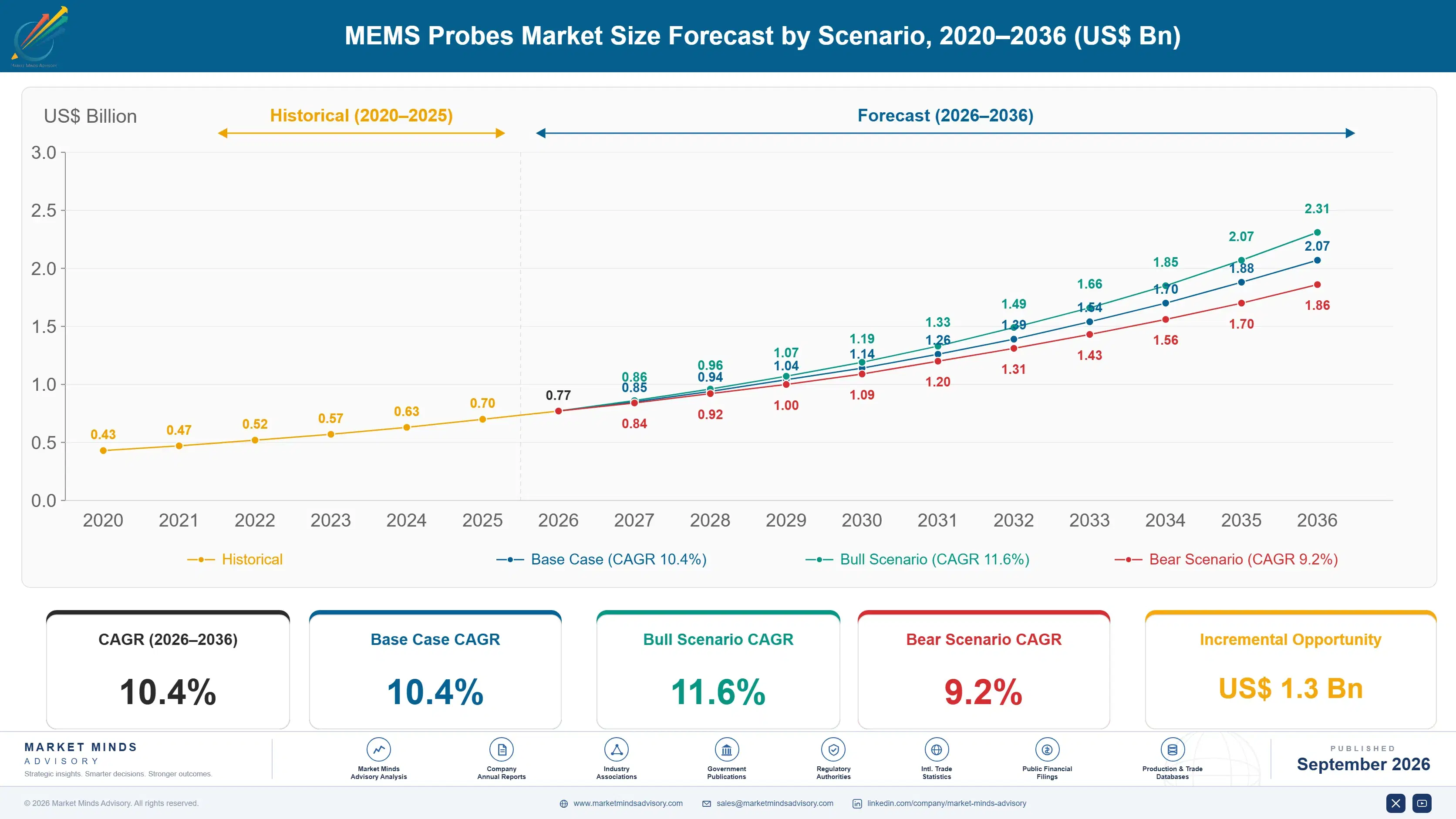
Between 2020 and 2025, MEMS probe demand grew steadily as semiconductor fabrication facilities pulled forward wafer-level test capacity across advanced logic and memory production, with pandemic-era supply disruption briefly slowing shipment timelines in 2021 and 2022. Vendors that had diversified their precision component supply chains ahead of the disruption recovered shipment schedules faster, a gap that persisted into 2023 before normalizing across most fabrication design cycles and component categories.
The base case assumes continued semiconductor fabrication capacity growth, sustained advanced packaging adoption, and rising high-frequency test requirements as foundries consolidate fragmented probing tools into unified test platforms across new fabrication nodes coming online worldwide. Probe card vendors and foundry test engineering teams are expanding vertical probe production capacity to support parallel qualification programs across multiple fabrication node transitions, a pattern MMA expects to persist through the forecast window. Investors increasingly favor this trend.
A strong bull case rests on accelerated advanced packaging adoption pulling forward probe card replacement cycles, while the primary bear risk is prolonged semiconductor capital expenditure delays in key markets that push out planned probe procurement by a year or more. Vendors positioned across standard and advanced packaging channels carry the least exposure to either scenario alone.

From Cantilever Contacts to Vertical Probe Arrays

MEMS probes sit at the center of semiconductor wafer-level test work across logic, memory, and analog device fabrication, and their design has moved decisively from simple cantilever contact structures toward high-density vertical probe arrays over the past decade. High-density vertical arrays deliver more contact points per unit area without the mechanical scrub damage common to older cantilever designs, mattering more as facilities push toward smaller contact pitches across widening wafer diameters.
MARKET CONCENTRATIONCR5 58%Top five vendors hold majority shipment volume share globally
AVERAGE SELLING PRICE$4,200Blended price across standard and advanced packaging probe tiers
TOP PRODUCING COUNTRYJapan 27%Reflects concentrated precision manufacturing and semiconductor equipment expertise
FINE-PITCH ADOPTION SHARE38% of shipmentsAdvanced packaging designs increasingly require sub-forty micron contact pitch
PROBE CARD LIFESPAN2 to 4 yearsHigh-density vertical probes typically outlast cantilever designs considerably overall
CONTACT RESISTANCE DRIFTUnder 5% annualAdvanced materials increasingly reduce degradation across repeated test cycles
Foundry demand tracks fabrication node transitions closely, since chipmakers both need to verify electrical performance and detect defects early before committing wafers to expensive downstream packaging and assembly processes. Contract test houses supporting foundry qualification are scaling probe sourcing accordingly, and several have begun offering probe refurbishment as a standalone cost-reduction service to fabs seeking to extend tooling life.
Advanced packaging integration follows a separate, faster-moving logic tied to chip stacking and heterogeneous integration trends, where probes increasingly test finer contact pitches at higher frequencies, and vendor selection favors probe cards with proven high-density architecture already built in. Automotive and industrial MEMS sensor testing represents a third, steadily growing demand pool, as device makers building harsh-environment sensors require probes capable of resolving contact reliability across production wafer lots.
"Probe vendors used to compete on contact reliability alone. Now the ability to test at ever finer pitch without damaging the wafer matters just as much as raw durability."
Director, Semiconductor Test and Wafer-Level Probing Practice · MMA Technology Practice · September 2026

Market Trends

Vertical Probe Arrays Displace Cantilever Contact Designs

Vendors are shifting product roadmaps decisively toward vertical probe arrays capable of delivering higher contact density without the mechanical scrub damage common to older cantilever designs. This matters increasingly as fabrication facilities push toward finer contact pitches to test increasingly compact chip designs across advanced fabrication nodes. FormFactor, Micronics Japan, and Technoprobe have each released new vertical probe card platforms in the past eighteen months, and foundry buyers in particular are specifying high-density vertical architecture as a mandatory qualification requirement rather than an optional feature for new fabrication test contracts.
Market Impact: Fabrication demand rises roughly 12% yearly

Advanced Packaging Integration Extends Vendor Revenue

Modern probe cards increasingly separate contact hardware from calibration and diagnostic software, letting foundries monitor probe wear and predict replacement timing rather than relying on fixed maintenance schedules. This shift is stretching probe card lifespans longer while opening a growing diagnostic software revenue stream for established vendors. MPI Corporation and Feinmetall both now generate a meaningful share of probe-related revenue from calibration software licenses sold well after the original probe card purchase, a trend MMA expects to accelerate through the forecast period. Smaller vendors lacking comparable software diagnostics increasingly struggle to match this expanded revenue stream.
Market Impact: Packaging demand grows 15% annually

Market Opportunities and Growth Drivers

Semiconductor Fabrication Capacity Growth Sustains Demand

Foundries continuing to expand fabrication capacity across multiple nodes need continuous probe card procurement across each new production line, sustaining steady demand well beyond the initial capacity ramp phase. Test engineering teams must requalify probe designs against each new fabrication node the foundry releases, and probe card vendors supporting this work are expanding vertical probe production capacity to keep pace. Taiwan, South Korea, and the United States are each expanding fabrication capacity simultaneously, giving vendors multiple overlapping regional demand waves rather than one single global adoption cycle to plan around.
Market Impact: Entry-level probe cards still exceed $8,000

Advanced Packaging Adoption Expands Test Requirements

Chipmakers across Taiwan, South Korea, and the United States are adopting chip stacking and heterogeneous integration packaging in response to rising performance demands, and this packaging work favors high-density vertical probes over traditional cantilever contact designs. Vendors with existing foundry certification and long-standing fabrication relationships capture a disproportionate share of this spending, since qualification cycles for new suppliers routinely stretch beyond eighteen months. MMA expects packaging-linked probe revenue to keep outpacing general standard test segment growth through most of the forecast period given current packaging trajectories. Commercial technology firms compete with probe vendors for limited packaging engineering talent.
Market Impact: Qualification cycles average over 18 months

Market Restraints and Challenges

High Probe Card Cost Limits Smaller Fab Access

Advanced vertical probe cards with fine-pitch, high-density contact arrays routinely cost well over fifty thousand dollars per card, pricing many smaller fabrication facilities out of leading-edge test capability. The root cause is the specialized precision manufacturing and material engineering these probe cards require, which do not benefit from consumer electronics manufacturing scale. Smaller fabs increasingly rely on outsourced test houses rather than purchasing dedicated advanced probe cards outright. Vendors are responding with tiered probe designs and leasing arrangements aimed at preserving access for budget-constrained facility segments. Larger fabs absorb this cost more easily given greater capital budgets.
Market Impact: Vertical probes reach 46% share

Long Foundry Qualification Cycles Delay Revenue Recognition

Foundry qualification for new probe card suppliers routinely stretches beyond eighteen months, driven by extensive contact reliability testing, thermal cycling, and layered fabrication approval processes that consumer electronics buyers never face. This root cause locks out newer entrants regardless of technical merit, concentrating foundry revenue among a handful of long-qualified incumbent vendors. The commercial impact is a widening gap between smaller specialist vendors and established players with existing foundry relationships. Some smaller vendors are pursuing subcontractor arrangements with qualified prime suppliers as a mitigation pathway around the direct qualification barrier.
Market Impact: Diagnostic software now adds 13% revenue
3 additional market trends, 4 additional growth drivers, and 3 additional restraints and challenges are covered in the full report. Contact sales@marketmindsadvisory.com to access the complete intelligence.

Segment CAGR and Growth Architecture

The market splits across six segments defined by contact architecture, spanning legacy cantilever probes through modern vertical and MEMS-based high-density arrays. MEMS-based vertical probe cards are pulling share fastest as advanced packaging demands finer contact pitch across fabrication nodes. Cantilever probe cards follow close behind as legacy analog device testing sustains steady demand from established fabrication facilities.
mems-probes-market-market-share-analysis-1789984985371

MEMS-Based Vertical Probe Cards

MEMS-based vertical probe cards are growing fastest, at roughly 15.6% annually, about 1.50 times the overall market rate. Demand concentrates in advanced packaging test, chip stacking validation, and fine-pitch fan-out wafer level packaging, where high-density contact meaningfully reduces test cycle time across production wafer lots. FormFactor, Micronics Japan, and Technoprobe have each committed significant research spending to widen contact density and improve signal integrity simultaneously, since the two capabilities traditionally traded off against each other in earlier probe card generations sold throughout the previous decade. This segment also commands the highest average selling price across the entire probe category, supporting healthier vendor margins even as overall unit volume growth trails the broader semiconductor test market.
CAGR 15.6%

Cantilever Probe Cards

Cantilever probe cards form the largest but slower-growing segment, driven by facilities testing legacy analog and mixed-signal devices that do not require fine-pitch vertical contact architecture. Rising fabrication cost pressure means more facilities delay full vertical migration per test line, since each new installation requires compatibility confirmation before production validation. Vendors including MPI Corporation and Feinmetall have narrowed the reliability gap between cantilever and vertical probes considerably, letting smaller fabs access precision once reserved for premium fabrication facilities. Manufacturing cost efficiency and durability increasingly differentiate competing cantilever designs, since fabs often need to certify distinct probe specifications across multiple parallel test lines simultaneously. MMA expects this gap to narrow further as vertical tooling matures across the industry.
CAGR 6.2%
Full segment breakdown across 6 segments available in the complete report.

Regional Architecture and Country Demand Map

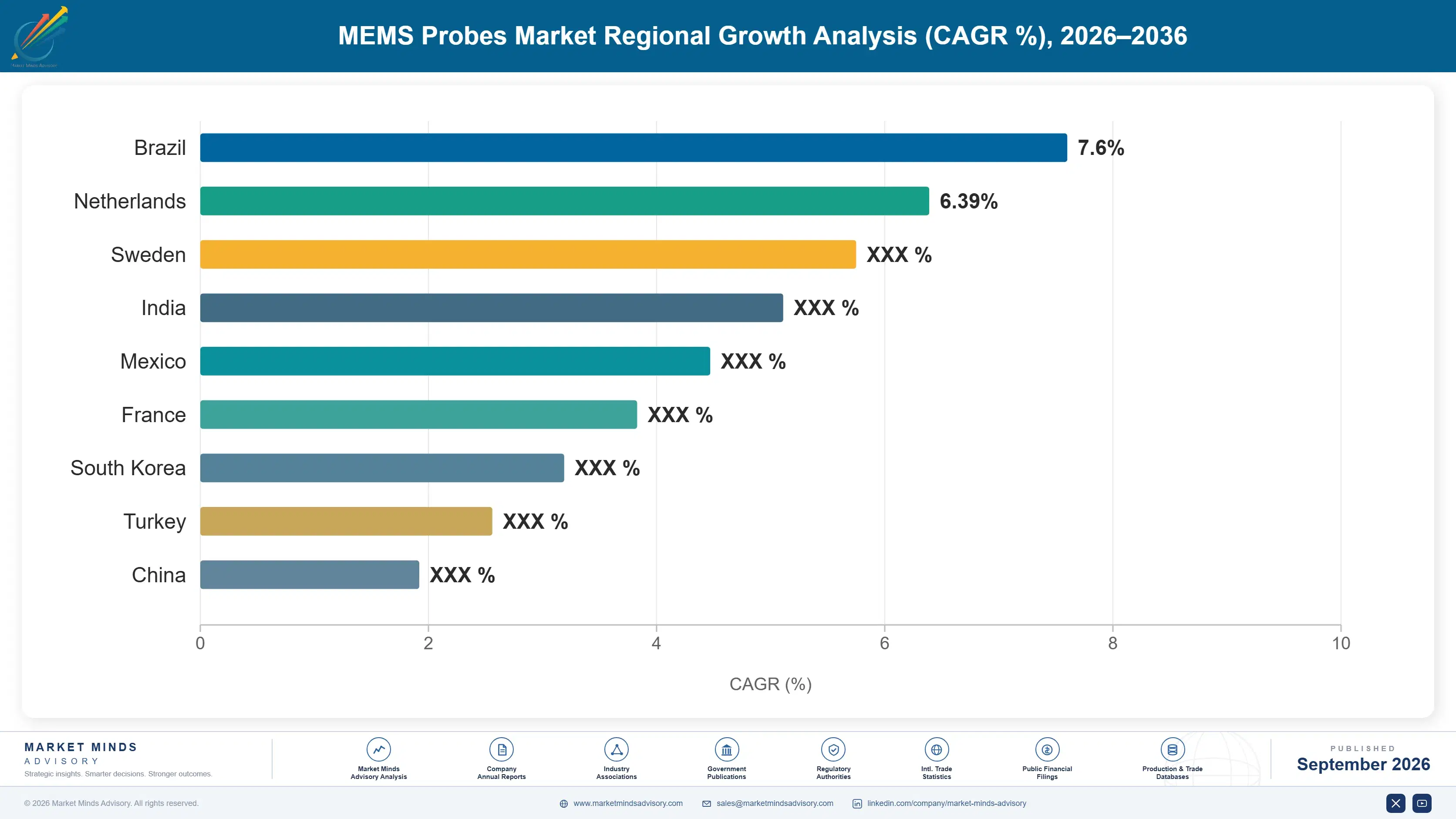
East Asia leads on concentrated semiconductor fabrication capacity across Taiwan, South Korea, and Japan, while North America follows closely on probe card design leadership and equipment vendor headquarters presence. South Asia and Pacific posts the fastest regional growth as India expands semiconductor test capacity from a smaller installed base.

North America

Probe card design leadership and semiconductor equipment vendor headquarters presence anchor North American demand, with the United States maintaining the largest single concentration of test engineering centers and fabrication design relationships across multiple chipmakers. FormFactor maintains headquarters and primary engineering operations here, giving domestic foundries faster feature access and direct support relationships unavailable to overseas competitors. Advanced logic and memory fabrication capacity expansion adds a second steady demand pool, particularly around leading-edge node qualification and test certification work. MMA counted 34 active foundry test contracts referencing vertical probe specifications during 2025 alone. Canada adds a smaller but stable demand pool through its own semiconductor test adoption and equipment programs administered separately from United States procurement cycles.
Share: 25% | CAGR: 11.5% (2026 to 2036)

Western Europe

German and French semiconductor equipment manufacturers anchor regional demand through automotive and industrial chip test certification requirements. Feinmetall, headquartered in Germany, holds a dominant regional design and engineering presence that smaller competitors struggle to match on precision manufacturing depth. Automotive-grade chip test segment concentration adds a distinct regional demand pool, since German fabrication facilities increasingly validate advanced probe systems against tightening European quality certification standards. Growth trails East Asia and North America here mainly because fabrication capacity expansion across the region proceeded more slowly than in leading Asian and American markets. Nordic countries add a smaller but technically sophisticated demand pool tied to specialty sensor fabrication programs supporting the region's growing MEMS device investment.
Share: 18% | CAGR: 9.0% (2026 to 2036)
Regional intelligence for 5 additional markets available in the complete report: East Asia, South Asia and Pacific, Latin America, Middle East and Africa, Eastern Europe. Contact sales@marketmindsadvisory.com.
mems-probes-market-country-cagr-analysis-1789984985884

Diagnostic Software Extends Probe Revenue Life

Probe card vendors are extracting more lifetime revenue per design win through calibration software licensing, refurbishment services, and premium high-density tiers rather than relying solely on the original hardware sale to generate margin. Margins vary widely across each pathway depending on fabrication segment and node scale. Margin economics vary widely across each pathway and fabrication tier.

Calibration Software Licensing Growth Expansion Program

Vendors including MPI Corporation and Feinmetall now sell probe wear diagnostic and calibration software as separate licensed add-ons to base probe card hardware, letting foundries add predictive maintenance capability incrementally rather than replacing entire probe fleets. This model has expanded software-attributable revenue to roughly 13% of total probe-related sales for leading vendors, with particularly strong uptake among foundries operating high-volume production lines. Subscription renewal rates for these software licenses now exceed 77% annually among established foundry accounts, giving vendors a highly predictable recurring revenue stream that partially offsets slower unit growth.
Market Impact: Software revenue now reaches roughly 13% of sales

Probe Refurbishment and Maintenance Service Program

Vendors are bundling multi-year refurbishment and maintenance contracts directly into new probe card sales, converting a traditionally separate aftermarket service into locked-in recurring revenue from the point of purchase. These bundled contracts now cover roughly 39% of newly sold foundry probe fleets, up meaningfully from levels seen five years earlier. Vendors report lower churn among accounts holding bundled agreements compared to those procuring refurbishment separately. Customers gain predictable maintenance costs and priority turnaround, while vendors gain multi-year visibility into service revenue and stronger foundry retention. Vendors report lower churn among accounts holding these bundled agreements over time.
Market Impact: Bundled contracts now cover roughly 39% of sales

High-Density Vertical Probe Premium Pricing Programs

Vendors offering fine-pitch, high-density vertical probe architecture command a substantial price premium over standard cantilever equivalents, often exceeding 33% above comparable base specifications. This premium reflects both the specialized precision engineering required and the smaller production volumes involved relative to standard probe lines. Foundries generally accept this premium given the yield improvement benefits involved for advanced packaging test, and vendors with established vertical probe expertise face limited price competition since few competitors can match the same reliability track record. Vendors keep investing in this engineering since margin expansion outweighs added production complexity and material costs involved.
Market Impact: Vertical probes now command a full 33% premium

Foundry Equipment Partnership and Deployment Programs

Leading vendors are establishing partnership programs with fabrication equipment integrators, providing preferential pricing and priority engineering support in exchange for guaranteed volume commitments and exclusive qualification arrangements. These partnerships expand vendor reach into smaller foundries who cannot justify direct probe evaluation, while generating steady wholesale revenue and valuable market intelligence on emerging fabrication requirements. Roughly 20% of total probe shipment volume now flows through such partnership channels rather than direct foundry sales, a share MMA expects to keep expanding as outsourced test integration gains broader acceptance. Vendors view these arrangements as a channel for reaching smaller cost-sensitive foundry customers.
Market Impact: Partnership channels now carry roughly 20% of shipments

Who Controls the Margin Pool

FormFactor, Micronics Japan, Technoprobe, MPI Corporation, and Feinmetall together hold roughly 58% combined shipment share, with FormFactor and Micronics Japan forming a leading tier ahead of remaining challengers on manufacturing scale and foundry design relationships. The gap between the top two vendors and the third-ranked challenger has widened as FormFactor and Micronics Japan invested more heavily in vertical probe research than smaller competitors could match.
Competitive activity currently centers on vertical probe density expansion, calibration software rollout, and advanced packaging design win competition, as vendors race to lock in long-cycle foundry contracts before rivals can complete their own qualification processes across multiple fabrication nodes. Several vendors announced expanded calibration software programs this year, converting one-time hardware sales into recurring revenue streams that improve retention against competitive displacement during future replacement cycles.

Rankings could shift meaningfully if a well-funded software-native entrant achieves foundry qualification faster than expected, or if advanced packaging demand growth outpaces the traditional standard test segment enough to reward vendors with deeper Taiwanese foundry relationships over the coming several years. Fabrication equipment integrators are gaining influence as intermediaries, since their qualification decisions shape which vendors reach smaller foundry customers lacking direct procurement relationships with established manufacturers.
mems-probes-market-company-positioning-matrix-1789984986424

Competitive Moat and Risk Dimensions

FORMFACTOR

Moat: Broad Advanced Node Portfolio

FormFactor's portfolio spans probe technology across nearly every advanced logic and memory fabrication node, letting the company serve customers from mature nodes through leading-edge production without ceding any single segment to specialized competitors lacking comparable breadth. This breadth lets FormFactor bundle probe cards across node generations into single foundry procurement contracts, an advantage smaller vendors cannot easily match.
FORMFACTOR

Risk: Premium Pricing Vulnerability

FormFactor's premium pricing across most product lines leaves room for lower-cost challengers like Taiwanese domestic suppliers to win price-sensitive mature-node accounts, particularly among smaller foundries with constrained capital budgets. FormFactor has responded by expanding lower-cost product tiers, though full cost competitiveness typically takes considerably longer than the pricing adjustments themselves.
MICRONICS JAPAN

Moat: Deep Precision Manufacturing Expertise

Micronics Japan maintains decades of precision manufacturing expertise across fine-pitch contact engineering, giving the company privileged access to leading-edge qualification processes that newer entrants find difficult to replicate within any reasonable competitive timeframe. This precision advantage also feeds directly into faster qualification approval for new fine-pitch contact designs, reinforcing its reputation among leading-edge foundry customers.
MICRONICS JAPAN

Risk: Limited Software Platform Depth

Micronics Japan's hardware-centric focus leaves its diagnostic software and analytics capability thinner than competitors like FormFactor, who have invested more heavily in calibration software platforms that extend probe card lifetime value. Micronics Japan has responded by partnering with software firms, though full platform integration typically takes considerably longer than the partnership agreements themselves.

Players Tracked

Prominent Players

FormFactor
Micronics Japan
Technoprobe
MPI Corporation
Feinmetall

Other Key Players

Japan Electronic Materials
Will Technology
Winway Technology
MJC Probe Inc
Celadon Systems
Cohu Inc
Advantest Corporation
Teradyne Inc
Chunghwa Precision Test Tech
Star Technologies
Kyoshin Electric
Wintest Corporation
Aehr Test Systems
SUSS MicroTec
ISC Co Ltd

Recent Developments

JANUARY 2026

FormFactor launched a new vertical probe card platform supporting fine-pitch fan-out wafer level packaging test applications, targeting foundries investing in next-generation advanced packaging capability ahead of upcoming fabrication node transitions. The platform reflects sustained vendor confidence in continued advanced packaging adoption despite lengthy foundry evaluation cycles.
Signal: Signals continued vendor investment in advanced packaging test capability industry-wide. across the broader semiconductor probe and wafer test industry.
SEPTEMBER 2025

Micronics Japan completed an acquisition of a smaller software analytics firm specializing in automated probe wear prediction, strengthening its diagnostic software portfolio and accelerating its shift toward recurring licensing revenue. The deal reflects a broader strategy of embedding proprietary prediction tools as a differentiator over pure hardware specifications.
Signal: Signals an accelerating vendor shift toward software-driven recurring revenue across the industry. as recurring software licensing gains broader acceptance.
APRIL 2025

Technoprobe announced an expanded manufacturing capacity investment at its Italian production facility to support growing foundry test demand across the region, adding dedicated production lines for its vertical probe family. The investment reflects confidence that regional semiconductor test demand will keep outpacing overall market growth through the decade.
Signal: Signals growing vendor confidence in sustained European semiconductor test demand growth. as manufacturing capacity investment keeps expanding regionally.

Precision Tungsten Alloy Cost Exposure

Precision tungsten alloy contact materials and specialized ceramic substrates together account for roughly 31% of probe card cost of goods sold, with much of that specialized material supply sourced from a small number of processors concentrated in Japan and China. Component lead times for these specialized materials run longer than for standard consumer-grade materials, forcing vendors to carry larger safety stock inventories to protect foundry delivery commitments.
A 2024 export control tightening on advanced tungsten processing equipment, reported in China's Ministry of Commerce disclosures, briefly slowed delivery of leading-edge contact materials used in newer vertical probe architectures, pushing some vendor lead times out by several months during the transition period. Vendors reported delivery delays of six to ten weeks on certain materials, according to FormFactor Investor Day disclosures, before alternative supply restored more normal delivery timelines by early 2025.

Smaller vendors lacking long-term supply agreements absorb this volatility more directly than FormFactor or Micronics Japan, both of which maintain diversified sourcing relationships and larger negotiated volume commitments that smooth through short-term disruptions. This gap compounds over successive product generations, since smaller vendors pass cost volatility to customers through less predictable pricing, weakening their position against rivals offering steadier contract pricing.
mems-probes-market-cost-volatility-analysis-1789984986619

Diversified Multi-Foundry Component Sourcing Agreements

Leading vendors qualify contact materials from multiple processors simultaneously rather than depending on a single supplier, letting them redirect orders quickly when one source faces capacity constraints or export restrictions without halting production entirely. This approach adds qualification overhead but has proven its value during recent supply disruptions, particularly for vendors serving foundry customers who cannot tolerate delivery delays.

In-House Contact Material Design Capability

Some vendors, particularly FormFactor and Micronics Japan, design specialized contact materials internally and outsource only processing, retaining design control that shortens qualification cycles when switching between material partners during supply disruptions across component categories. This model costs more upfront in research spending but pays off during supply shocks, since vendors requalify a supplier in weeks rather than months rivals require.

Long-Term Volume Purchase Commitments

Vendors increasingly negotiate multi-year volume purchase commitments with key material suppliers in exchange for priority allocation during shortages, trading pricing flexibility for greater delivery certainty across critical contact material supply used in production probe cards. These agreements typically span three to five years, giving vendors production planning certainty even when broader material market conditions turn volatile.

Portfolio Architecture for Margin Defence

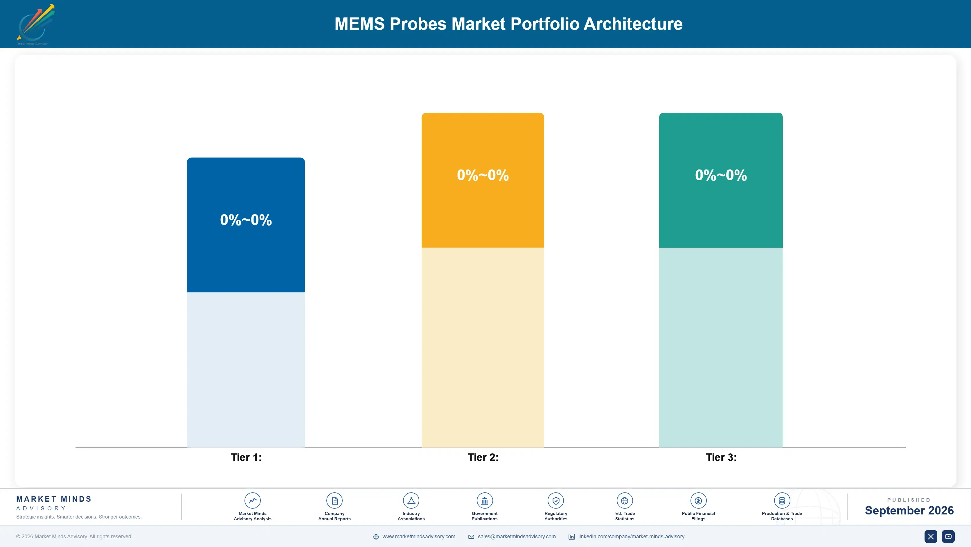
The market splits into three commercial tiers, running from commodity cantilever probes used for basic mature-node testing through premium vertical probe platforms qualified for advanced packaging work, each carrying distinctly different margin economics. Gross margin ranges span roughly twenty-two percentage points between the lowest and highest tiers, reflecting how much specialized precision engineering and contact density capability separates a basic cantilever probe from a premium vertical platform sold to leading-edge foundries.
Volume tier products compete mainly on price against Taiwanese and low-cost Asian manufacturers, while premium and packaging-integrated tiers command significantly stronger gross margins that reflect specialized engineering and lengthy customer qualification barriers protecting incumbents. Vendors serving the volume tier increasingly struggle to sustain healthy margins as Taiwanese manufacturers improve product specifications while undercutting established western pricing on comparable base-level probe capability across most commercial applications.

High-value margin pools concentrate heavily in vertical probe modules and advanced packaging test platforms, where established vendor relationships and certification barriers keep new entrants locked out regardless of underlying technical capability offered. Vendors positioned across all three tiers capture strong overall economics, since volume tier sales fund research investment that sustains premium tier competitiveness over successive product generations well into the coming decade.

Basic cantilever probes for mature-node testing at smaller fabrication facilities, competing primarily on price against Taiwanese manufacturers offering comparable core specifications at meaningfully lower price points. Winway and Will Technology lead this tier on price.
Gross Margin

Vertical probe platforms qualified for advanced packaging certification, commanding stronger margins through contact density, signal integrity depth, and established customer qualification relationships. Technoprobe and MPI Corporation both compete strongly here.
Gross Margin

MEMS-based fine-pitch probe systems requiring extensive foundry qualification and chip stacking validation, carrying the strongest margins due to lengthy qualification barriers and limited competitive vendor pool. FormFactor holds particular strength in this emerging tier.
Gross Margin
mems-probes-market-portfolio-architecture-1789984987132

High-value Sub-segments and Strategic Watch-out

MEMS-Based Vertical Probe Cards

This segment combines the fastest unit growth with the strongest margins in the entire market, as foundries seeking advanced packaging test demand vertical capability regardless of price, making it the clearest strategic priority for vendor investment planning. MMA rates this the single highest priority watch item overall.

Cantilever Probe Cards

Mature-node test demand keeps expanding steadily as legacy fabrication capacity persists, and margins here remain healthy even though growth trails the vertical probe segment, making this a reliable secondary growth pool for vendors. Cost efficiency and reliability increasingly matter for smaller fabs testing legacy analog devices at scale.

Standard Wafer-Level Test Probes

This legacy architecture still anchors overall volume and revenue today, but growth has flattened as customers migrate toward vertical capability, making it the core installed base vendors must defend rather than expand aggressively. Vendors must manage this decline without losing valuable support revenue attached to it across the base.

MEMS Sensor Test Probe Modules

Embedded sensor test modules within larger fabrication test systems represent a smaller but strategically important niche, since losing this integration business could cascade into losing broader foundry relationships entirely over time. MMA flags this as a strategic watch-out given its influence on customer relationships and future contract renewals.

Design Wins Anchor Recurring Demand

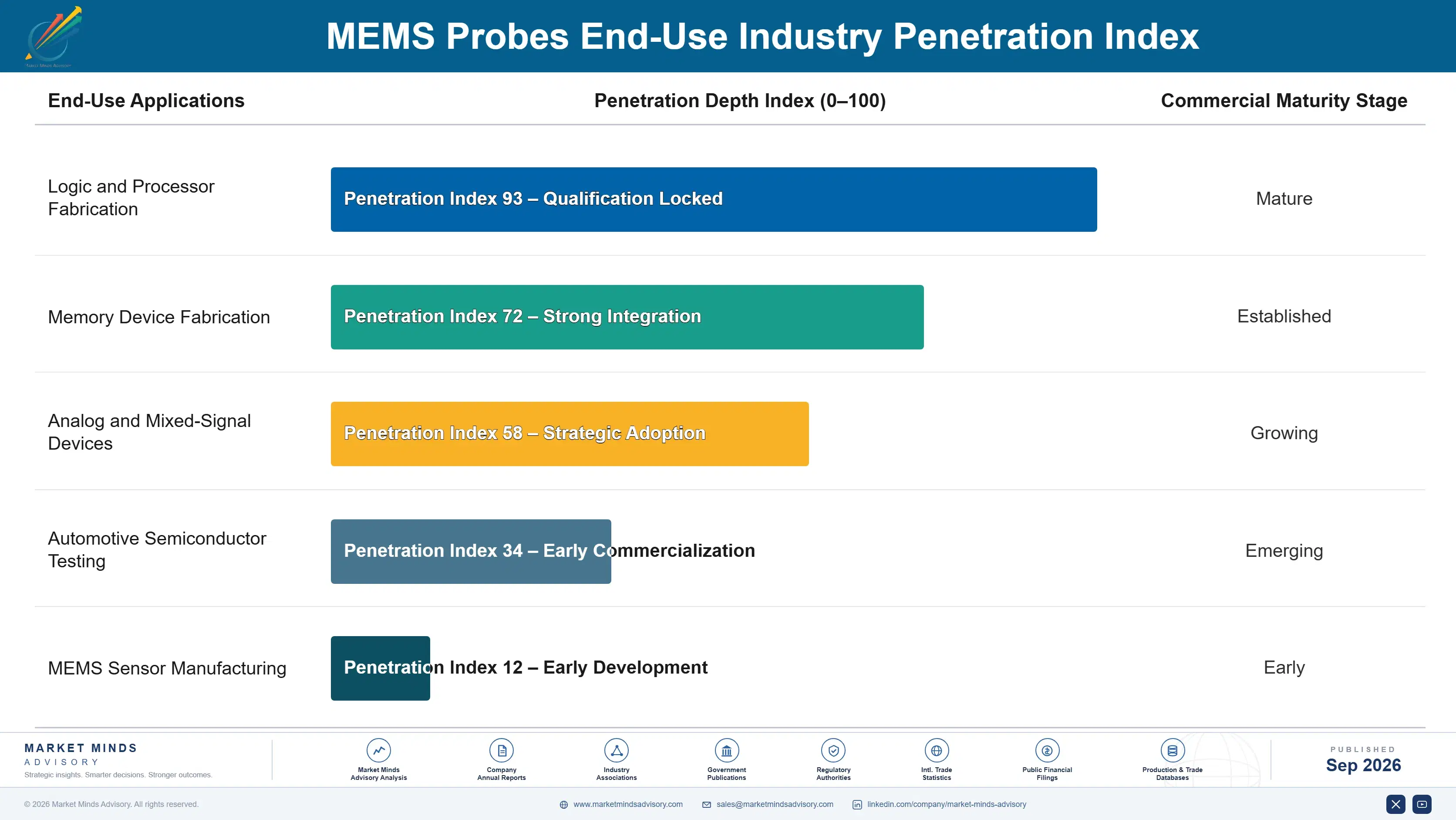
Probe card vendors increasingly earn recurring revenue through multi-year fabrication node design wins rather than depending solely on one-time hardware sales, since semiconductor production cycles typically span three to five years per node generation. This annuity-like revenue stream means vendors with the largest installed design win base enjoy a compounding advantage over smaller rivals, since each node win generates component revenue for a decade or more into the future.
Adoption depth varies meaningfully by end-use vertical: leading-edge foundries integrate probe cards deeply into locked qualification programs that resist vendor switching for years, while mature-node facilities rotate suppliers more frequently as pricing pressure evolves. Automotive and industrial chip customers sit between these extremes, replacing probe suppliers roughly every four to six years as qualification standards evolve, giving vendors a moderately predictable replacement cadence to plan around.

A generational shift in buyer profiles is underway as younger test engineers increasingly favor software-configurable probe systems over fixed-function hardware, valuing flexibility and remote diagnostic updates over the raw specifications that dominated purchasing decisions a decade earlier. Vendors that fail to modernize software interfaces risk losing these buyers to entrants offering cloud-connected diagnostic platforms, even when hardware performance remains competitive with established incumbent product lines.
mems-probes-market-end-use-penetration-index-1789984987616

Where Density Beats Raw Contact Count

These are among the four positions where our research anticipates prominent divergence between winners and laggards over the coming forecast period. Each is grounded in the demand model, the regulatory perimeter, and the announced capacity pipeline.
01 / VERTICAL PROBE INVESTMENT

Prioritize vertical probe density research now

MEMS-based vertical probe cards are growing at roughly 15.6% annually, about 1.50 times the overall market rate, and foundries already treat high-density contact as a mandatory qualification requirement. Vendors delaying this investment risk losing design wins to FormFactor and Micronics Japan, both of which have already committed significant research spending toward wider contact density and improved signal integrity. The window for smaller challengers to close this technical gap is narrowing each year, and it will likely close entirely within the next several forecast cycles.
02 / SOFTWARE LICENSING EXPANSION

Build recurring software revenue streams deliberately

Software licensing already contributes a full roughly 13% of total probe-related revenue for leading vendors, and this share keeps expanding steadily as foundries increasingly value predictive maintenance capability over reactive probe replacement. Vendors that fail to build comparable licensing infrastructure will keep depending entirely and indefinitely on hardware sales cycles for revenue, ceding recurring revenue advantages to more sophisticated rivals. This gap will only widen as foundries grow ever more comfortable with subscription-based diagnostic software across every fabrication node worldwide.
03 / FOUNDRY QUALIFICATION PROGRAMS

Pursue foundry qualification despite long timelines

Foundry qualification cycles routinely exceed a full eighteen months, but the resulting design wins lock in stable, high-margin revenue that consumer electronics customers rarely match given their shorter replacement cycles and considerably greater overall price sensitivity. Vendors already holding qualification certifications and established foundry relationships capture a disproportionate share of this spending, making early qualification investment critical despite the multi-year payback period involved. Newer entrants should consider subcontractor arrangements with qualified prime suppliers as a faster, lower-risk entry pathway into this segment.
04 / REGIONAL MANUFACTURING POSITIONING

Expand Taiwanese manufacturing and design capacity

Taiwan's semiconductor fabrication demand is growing meaningfully faster than the broader overall global market, driven by aggressive government-backed advanced packaging investment across the country specifically and sustained capacity expansion across allied East Asian foundry supply chains simultaneously and steadily. Vendors lacking a strong regional manufacturing and design presence risk steadily losing share to established suppliers, which maintain deep domestic manufacturing relationships throughout the region. Establishing local design infrastructure now positions vendors well ahead of the next fabrication capacity expansion wave across the region.

Engagement Snapshot From the Field

A live engagement with an industry participant carrying material or product regulatory and market exposure ahead of a defining policy shift, showing how our research translates into a defensible multi-year portfolio strategy.
MARKET MINDS ADVISORY · CLIENT ENGAGEMENT SUMMARY
MEMS Probes Producer Strategic Portfolio Review and Transition Roadmap 2026·Investment Scenario on MEMS Probes Exposure Evaluation 2025-26
CLIENT PROFILE
The client operates a mid-size Taiwanese foundry expanding advanced packaging test capacity ahead of a new chip stacking production line launch, seeking a probe card vendor able to meet strict contact density and long-term design support requirements across a multi-year fabrication program. The foundry had relied on a single legacy vendor for over five years and wanted an independent, unbiased comparison before committing to a new multi-year supply relationship.
STRATEGIC CHALLENGE
The client needed to select a probe card vendor for a multi-year fabrication program but lacked internal expertise to compare contact density specifications, licensing terms, and design support depth across the small pool of eligible established suppliers. A poor vendor choice risked locking the foundry into unfavorable terms for the program's full duration with no practical opportunity to switch suppliers midway.
MMA APPROACH
MMA analysts benchmarked five qualified vendors on contact density capability, signal integrity flexibility, design support engineering track record, and existing foundry contract history, then modeled total lifetime program cost across a projected five-year probe deployment and support period. Analysts also interviewed program engineers directly to weigh qualitative factors such as technical support responsiveness that pure specification comparisons routinely overlook in vendor selection processes.
KEY FINDINGS
  1. The selected vendor's vertical architecture reduced projected five-year test cost by roughly 19% compared to the closest rival bid (client-reported, unverified by MMA).
  2. Contact density capability exceeded the program's minimum specification by a meaningful margin, providing headroom for future chip stacking generations without requiring probe replacement.
  3. Design support engineering depth proved decisive, since the winning vendor could resolve calibration requests within days rather than the weeks required by two competing bidders.
  4. The foundry completed vendor qualification approximately six weeks ahead of its internal program schedule, according to client-reported figures unverified by MMA, easing budget approval timing.
CLIENT PROFILE
The client operates a mid-size Taiwanese foundry expanding advanced packaging test capacity ahead of a new chip stacking production line launch, seeking a probe card vendor able to meet strict contact density and long-term design support requirements across a multi-year fabrication program. The foundry had relied on a single legacy vendor for over five years and wanted an independent, unbiased comparison before committing to a new multi-year supply relationship.
STRATEGIC CHALLENGE
The client needed to select a probe card vendor for a multi-year fabrication program but lacked internal expertise to compare contact density specifications, licensing terms, and design support depth across the small pool of eligible established suppliers. A poor vendor choice risked locking the foundry into unfavorable terms for the program's full duration with no practical opportunity to switch suppliers midway.
MMA APPROACH
MMA analysts benchmarked five qualified vendors on contact density capability, signal integrity flexibility, design support engineering track record, and existing foundry contract history, then modeled total lifetime program cost across a projected five-year probe deployment and support period. Analysts also interviewed program engineers directly to weigh qualitative factors such as technical support responsiveness that pure specification comparisons routinely overlook in vendor selection processes.
KEY FINDINGS
  1. The selected vendor's vertical architecture reduced projected five-year test cost by roughly 19% compared to the closest rival bid (client-reported, unverified by MMA).
  2. Contact density capability exceeded the program's minimum specification by a meaningful margin, providing headroom for future chip stacking generations without requiring probe replacement.
  3. Design support engineering depth proved decisive, since the winning vendor could resolve calibration requests within days rather than the weeks required by two competing bidders.
  4. The foundry completed vendor qualification approximately six weeks ahead of its internal program schedule, according to client-reported figures unverified by MMA, easing budget approval timing.
RECOMMENDED STRATEGY
Phase 1: Phase one: shortlist vendors meeting minimum contact density and foundry qualification specifications before evaluating pricing terms. This narrows the field quickly before deeper commercial evaluation begins. Phase 2: Phase two: model total five-year program cost, including diagnostic software licensing and support fees, not just the initial probe price. Phase 3: Phase three: negotiate multi-year design support and licensing agreements concurrently with the probe purchase to lock in pricing. These agreements protect against future component supply disruptions after launch stabilizes.
OUTCOME
The foundry selected a vendor offering materially lower projected lifetime test cost and completed qualification ahead of schedule, according to client-reported figures unverified by MMA, strengthening its competitive position for the underlying chip stacking production line launch. Program engineers specifically praised the vendor's calibration turnaround speed during the qualification testing phase that followed.

Frequently Asked Questions

Foundational context covering the market sizes, CAGR, scope, country, region and competition that inform every finding below. This section is provided to cover basics and most often pre-purchase conversations, answered from the MMA Primary Research Dataset.

What is the current size of the MEMS Probes Market?

The MEMS Probes Market reached roughly 0.68 billion dollars in 2025. Rising semiconductor fabrication capacity and expanding advanced packaging adoption are the primary drivers behind this current market scale.

How large will the MEMS Probes Market be by 2036?

MMA projects the market will reach approximately 2.02 billion dollars by 2036. That represents roughly 2.69 times its 2026 value, driven by sustained vertical probe and advanced packaging demand growth.

What is the CAGR for the MEMS Probes Market 2026 to 2036?

The market is projected to grow at a 10.4% compound annual rate between 2026 and 2036. This reflects steady standard test demand alongside faster-growing vertical probe procurement.

Which segment is growing fastest?

MEMS-Based Vertical Probe Cards are growing fastest, at roughly 15.6% annually, about 1.50 times the overall market rate. Foundries increasingly treat high-density contact as a mandatory qualification requirement.

Who are the major companies in the MEMS Probes Market?

FormFactor, Micronics Japan, Technoprobe, MPI Corporation, and Feinmetall lead the market. Together these five companies hold roughly 58% combined share on a shipment volume basis.

Which country is growing fastest?

Taiwan is growing fastest, at roughly 12.8% annually, as semiconductor fabrication capacity expands alongside aggressive advanced packaging investment. This is pulling component sourcing toward vendors with strong regional manufacturing networks.

Report Segmentation Architecture

The full report scope spans multiple orthogonal segmentation dimensions, with cross-tabulated demand data provided for each dimension pair. Coverage extends further to regional breakdowns, trend trajectories, and the competitive detail needed to support segment-level decision-making.

By Primary Market Dimension

  • Cantilever Probe Cards
  • MEMS-Based Vertical Probe Cards
  • Standard Wafer-Level Test Probes
  • MEMS Sensor Test Probe Modules
  • Fan-Out Wafer Level Packaging Probes
  • High-Frequency Test Probe Systems

By End-Use Industry

  • Logic and Processor Fabrication
  • Memory Device Fabrication
  • Analog and Mixed-Signal Devices
  • Automotive Semiconductor Testing
  • MEMS Sensor Manufacturing

By Commercial Dimension

  • Direct Foundry Design Win Sales
  • Fabrication Equipment Integrator Channels
  • Design Support Service Agreements
  • Refurbishment and Aftermarket Distribution

By Region

  • North America
  • Western Europe
  • East Asia
  • South Asia and Pacific
  • Latin America
  • Middle East and Africa
  • Eastern Europe

Scope, Methodology, and Coverage

Every figure in this report is reproducible from documented input assumptions. The scope below maps the historical period, the forecast horizon, the segmentation dimensions, and the countries covered, alongside the underlying primary and qualitative methodology.
Historical Period
2020 to 2025
Forecast Period
2026 to 2036
Base Year
2025 (USD billions; MMA Primary Research Dataset, September 2026)
Market Definition
This report covers probe cards and test contact devices used to electrically test semiconductor wafers and MEMS devices before die separation and packaging. It excludes standalone automated test equipment systems, final package-level test sockets, and general electrical connectors sold without integrated wafer-level probing capability.
Quantitative Units
USD billions, unit shipment volume where cited
Segmentation Dimensions
Contact architecture, end-use industry, commercial distribution channel
Regions Covered
North America, Western Europe, East Asia, South Asia and Pacific, Latin America, Middle East and Africa, Eastern Europe
Countries Covered
Taiwan, South Korea, Japan, United States, China, Germany, India
Key Companies Profiled
FormFactor, Micronics Japan, Technoprobe, MPI Corporation, Feinmetall
Quantitative Methodology
Primary survey, n=3,800 respondents, Q4 2025, six countries; demand-side model with trade association cross-validation
Qualitative Methodology
47 expert interviews, Q4 2025; applied to validate demand model assumptions, identify emerging dynamics, and assess competitive positioning
Report Format
PDF and XLSX data workbook (Word format preview document)
Publisher
Market Minds Advisory
Report Code
MMA-2026-TEC-223
Published
September 2026
Contact
sales@marketmindsadvisory.com | www.marketmindsadvisory.com

Purchase the full MEMS Probes Market Report (2026 to 2036).

This report gives procurement, engineering, and strategy teams a complete view of the MEMS Probes Market through 2036. It combines primary survey data from 3,800 respondents with 47 expert interviews to quantify segment growth, regional demand shifts, and competitive positioning. Readers get granular forecasts across six probe segments and seven regions, along with detailed profiles of the five leading vendors. The analysis also covers input cost exposure, portfolio margin economics, and emerging design-win pressure points shaping vendor selection decisions. It also flags where competitive rankings are most likely to shift.
Ten-year granular forecast across six segments
Full regional breakdown across seven markets
Five detailed competitor profiles with moat analysis
Input cost exposure and mitigation strategies
Portfolio tier margin economics and benchmarking detail
Anonymised client case study with strategy playbook

Built For The People Who Decide

From boardroom strategy to bench-side execution, this report is read cover-to-cover by leaders shaping the next decade of their industry, turning demand scenarios, market dynamics and valuation benchmarks into decisions.
CXOs/ Presidents/ VPs/ Managers
M&A and Corporate Development
Strategy Teams and R&D Heads
Procurement and Product Directors
Regulatory and Compliance Leaders
Investor Relations and Equity Analysts