Market Minds Advisory
Integrated CMOS Tri-gate Transistor Market

Integrated CMOS Tri-gate Transistor Market: Integrated CMOS Tri-gate Transistors: AI Chip Demand and the Race Toward the Next Transistor Architecture

Foundries racing to keep AI chip yields high on ever-smaller nodes are pushing tri-gate transistor architecture to its physical limits, forcing an industry-wide transition toward gate-all-around designs years ahead of schedule.

Lead Analyst

Published

September 2026

Make Smarter Decisions with Customized Research Insights

Request a free sample report and evaluate market opportunities, growth trends, and competitive dynamics relevant to your business needs.

2025 MARKET VALUE$14.2BMarket Size 2025
2036 FORECAST VALUE$43.0BBase Case , 2026 to 2036
CAGR 2026 TO 203610.6 %Bull 11.9% / Bear 9.3%
INCREMENTAL OPPORTUNITY$27.3BNet 10- year value creation
EXPANSION MULTIPLE2.74x2036 value over 2026 base
Strategic Levers
M&A Pipeline
Regional Outlook
Country Rankings
Competitive Intelligence
Segmental Deep-dive
Call-Us : 91 93563 13602

Executive Snapshot and Market Trajectory.

Foundries are discovering that tri-gate transistor architecture cannot scale much further without hitting physical leakage and power limits, and that ceiling is now the single clearest signal of which manufacturers will lead the next process-node transition across the entire global semiconductor industry today and tomorrow.
AI accelerator and GPU chip demand is pulling tri-gate transistor production toward the most advanced process nodes, and East Asian foundries are moving fastest, backed by the deepest concentration of leading-edge manufacturing capacity anywhere in the world today, while North American chip designers add a second, rapidly scaling pool of demand for the most advanced available process nodes on the market today and well into the future.
Competitive character is shifting from a pure process-node scaling race toward a broader packaging and architecture-innovation contest, and legacy foundries that built moats around node leadership are racing to develop gate-all-around transistor capability before rivals capture the next generation of advanced chip contracts outright, a shift that export-control restrictions and mounting geopolitical supply chain tension are both complicating considerably faster than most incumbents had originally expected just a couple of years ago now.
Market Definition
The integrated CMOS tri-gate transistor market covers semiconductor chips fabricated using three-dimensional tri-gate, or FinFET, transistor architecture across all process nodes and end-use applications. It excludes planar transistor chips fabricated on older process technology and next-generation gate-all-around transistor chips not yet in volume commercial production.
Base Year Value
$14.2B in 2025 (MMA Primary Research Dataset, September 2026)
Forecast Period
2026 to 2036, eleven discrete annual values
CAGR
10.6% base case. Bull 11.9%. Bear 9.3%.
Fastest Growth Segment
AI Accelerator and GPU Chips: 18.0% CAGR
Fastest Growth Country
Taiwan: 15.2% CAGR
Fastest Growth Region
South Asia and Pacific: 12.6% CAGR
Largest Region
East Asia: 30% of 2025 global value
Market Leaders
TSMC, Intel, Samsung Electronics, GlobalFoundries, and United Microelectronics Corporation lead the market. Source: MMA Primary Research Dataset, July 2026.
Primary Survey
n=3,800 procurement and R&D decision-makers, Q4 2025, six countries
Methodology
Demand-side build-up, cross-validated against public data, 47 expert interviews

Integrated CMOS Tri-gate Transistor Market Forecast Scenarios

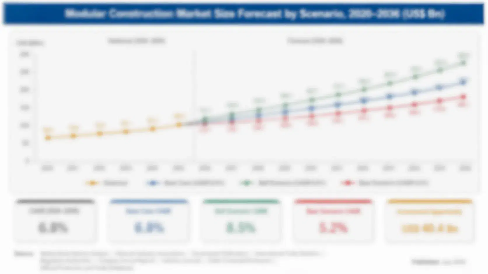
integrated-cmos-tri-gate-transistor-market-size-forecast-scenario-1788851837113
Between 2020 and 2025 the market grew at an estimated 9.6 percent annual clip as foundries scaled tri-gate transistor production across mainstream mobile and computing process nodes worldwide and across every major chipmaking region, though most advanced-node capacity at that time still served consumer electronics rather than the AI accelerator workloads driving demand today across the industry.
The base case assumes 10.6 percent annual growth through 2036, driven by three mechanisms: AI accelerator and GPU chip demand pulling production toward the most advanced tri-gate process nodes available today, automotive and industrial electronics adopting more advanced chip architecture as vehicles add more compute-intensive features each year and model cycle, and foundries expanding leading-edge capacity to meet demand that traditional planar transistor technology could no longer economically serve at scale.
The bull case turns on AI chip demand accelerating faster than current foundry capacity roadmaps assume, pulling forward advanced-node capacity expansion industry-wide well ahead of current vendor plans and annual budget cycles. The bear case centers on the gate-all-around transistor transition arriving faster than expected, considerably shortening the commercial window remaining for tri-gate architecture across the board.

From Tri-Gate Scaling to the Gate-All-Around Transition

Foundries that spent a decade perfecting tri-gate transistor manufacturing at successively smaller nodes are now confronting the physical limits of that architecture head-on across the entire global industry, and vendors that can extend tri-gate economics while preparing gate-all-around capacity are capturing the largest share of new advanced-node contracts across nearly every major chip designer relationship tracked in this report today.
TOP-FIVE VENDOR CONCENTRATION62%Combined revenue share held by the leading global foundries
AVERAGE ADVANCED-NODE WAFER ASP$18,500Blended selling price for a leading-edge finished silicon wafer
LEADING MANUFACTURING HUB SHARE68%Share of global advanced wafer output concentrated in one economy
LEADING-EDGE CAPACITY UTILIZATION96%Share of installed advanced-node production capacity currently running
PROCESS NODE TRANSITION CYCLE3 yearsTypical interval between successive advanced process node generations
MATURE NODE YIELD RATE94%Typical proportion of functional chips produced per wafer batch
Commercial activity concentrates around large, multi-year foundry capacity agreements with major chip designers rather than smaller, one-off wafer orders, since an advanced-node manufacturing relationship typically locks a customer into a single foundry's process design kit for years given the substantial engineering cost of redesigning chips for a competing node and requalifying the entire supply chain from scratch across every affected product line and market.
Over the next decade, the decisive forces will be the transition timeline toward gate-all-around transistor architecture that will eventually supersede tri-gate designs entirely across the industry, export-control policy that fragments which customers can legally access the most advanced nodes available today, and rising capital costs for each successive fabrication facility generation that only the very largest foundries can realistically afford to build.
"The foundries losing the next generation of contracts aren't the ones with worse tri-gate yields. They're the ones with no credible answer for what comes after."
Director, Semiconductor Process Technology Practice · MMA Technology Practice · September 2026

Market Trends

Gate-All-Around Transition Reshaping Long-Term Foundry Roadmaps

Leading foundries are simultaneously operating mature tri-gate production lines while ramping gate-all-around transistor capacity for the next process-node generation, creating a transitional period where both architectures coexist across different customer contracts and product lines. This dual-architecture period is forcing foundries to maintain two parallel engineering organizations and qualification pipelines rather than a single unified roadmap, raising operating costs during the transition considerably. Foundries that manage this transition smoothly are retaining customer relationships across both architecture generations, while those that stumble risk losing customers to competitors further along the gate-all-around ramp.
Market Impact: Adds 2.1 billion automotive-grade chip units
AI Chip Demand Concentrating Capacity at the Most Advanced Nodes

AI accelerator and GPU manufacturers are absorbing an outsized share of the most advanced tri-gate process node capacity available, crowding out other customers who previously had easier access to leading-edge manufacturing slots across the industry. This concentration is forcing chip designers in automotive, networking, and other sectors to either accept longer lead times or settle for less advanced process nodes than they originally planned to use for new product lines. Foundries are responding by prioritizing capacity allocation toward the highest-margin AI accelerator contracts, further squeezing availability for lower-margin customer segments.
Market Impact: Extends 68 percent leading-edge share

Market Opportunities and Growth Drivers

Automotive Electronics Demanding More Advanced Chip Architecture

Modern vehicles are incorporating substantially more compute-intensive features, including advanced driver assistance and in-vehicle AI processing, that require tri-gate transistor-based chips rather than the older planar technology automotive electronics traditionally relied upon for decades in production. Automotive customers historically preferred mature, well-proven process nodes over leading-edge technology given the industry's extreme reliability requirements, but that preference is shifting as compute demands within the vehicle continue rising. Foundries with automotive-qualified tri-gate process nodes are winning disproportionate share of this transitioning demand ahead of competitors still focused primarily on consumer and computing customers.
Market Impact: Raises fab construction costs 22 percent

Taiwan's Advanced Packaging Investment Extending Foundry Leadership

Taiwan's leading foundries are investing heavily in advanced packaging technology that extends the performance benefits customers can extract from tri-gate transistor chips without requiring a full node transition, effectively squeezing additional value out of existing process technology across multiple successive product generations and design cycles alike. This packaging investment is reinforcing Taiwan's position as the preferred manufacturing location for the most demanding chip designs, since customers increasingly select a combined wafer fabrication and packaging solution from one location rather than coordinating across separate suppliers in different countries and time zones.
Market Impact: Limits further scaling beyond 3 nanometers

Market Restraints and Challenges

Rising Fabrication Facility Capital Costs Limiting New Entrants

Each successive generation of advanced tri-gate fabrication facility costs substantially more to build than the previous generation, and that escalating capital requirement has effectively limited the number of companies capable of competing at the most advanced process nodes to a small handful of the largest foundries worldwide. The root cause is that equipment costs for extreme ultraviolet lithography and advanced packaging tools have risen faster than the revenue growth most chipmakers can generate from a single facility. Vendors are mitigating the burden by forming joint-venture fabrication partnerships and pursuing government subsidy programmes that share construction costs across multiple stakeholders.
Market Impact: Adds $2.6 billion transition-period capex

Approaching Physical Limits Constraining Further Tri-Gate Scaling

Tri-gate transistor architecture is approaching fundamental physical limits around current leakage and power density that make further scaling within the same basic design increasingly difficult and expensive to achieve at any meaningful scale. The root cause is that shrinking transistor dimensions further increases quantum tunneling effects that tri-gate geometry cannot fully suppress the way newer gate-all-around designs can suppress them instead. Vendors are mitigating the constraint by accelerating gate-all-around transistor development while extending tri-gate life through advanced packaging and materials innovations that defer the need for a full architectural transition.
Market Impact: Absorbs 44 percent of leading-edge capacity
3 additional market trends, 2 additional growth drivers, and 4 additional restraints and challenges are covered in the full report. Contact sales@marketmindsadvisory.com to access the complete intelligence.

Segment CAGR and Growth Architecture

This report segments the market by end-use application rather than by process node alone, since the same underlying tri-gate transistor technology typically serves computing, mobile, automotive, and networking buyers through different chip designs built on comparable manufacturing platforms and equipment across the industry. Six application segments capture how demand concentrates across different performance and cost requirements.
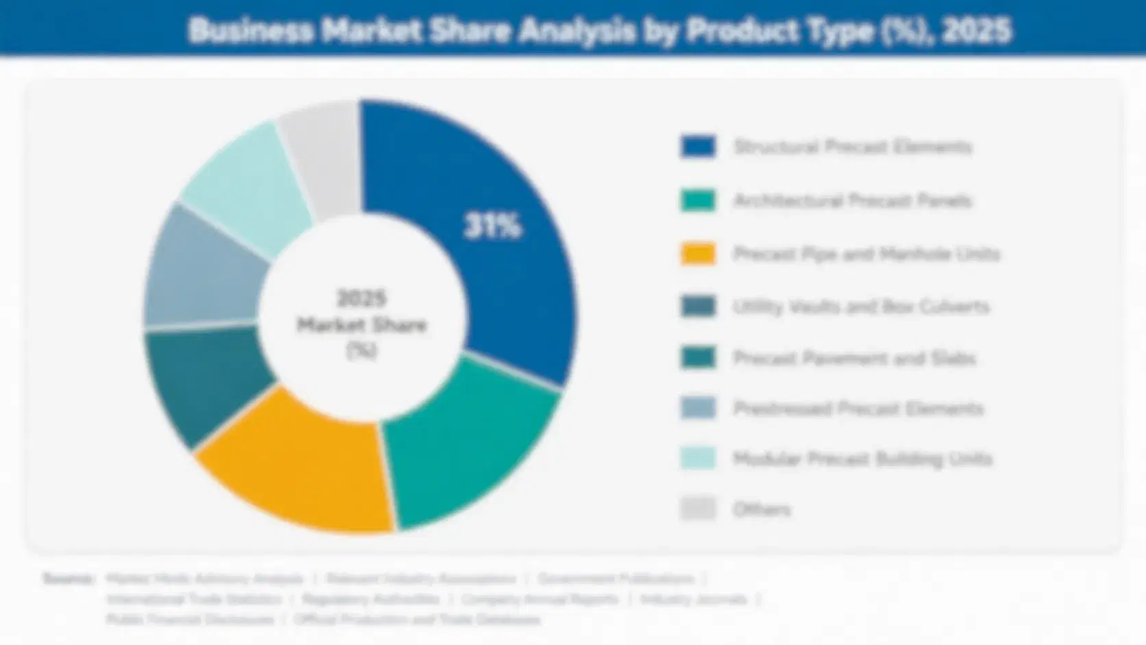
integrated-cmos-tri-gate-transistor-market-market-share-analysis-1788851837427

AI Accelerator and GPU Chips

AI accelerator and GPU chips are growing fastest because hyperscalers and enterprises are racing to build out training and inference infrastructure that requires the most advanced tri-gate process nodes available anywhere in the world today and for the foreseeable future ahead of any competing capital priority whatsoever. These chips command premium pricing and priority capacity allocation from foundries, since the revenue per wafer from an AI accelerator vastly exceeds that of a comparable wafer used for mobile or general-purpose computing chips. Foundries are increasingly reserving their most advanced capacity specifically for this segment, sometimes at the expense of other customer categories that previously had easier access to leading-edge manufacturing slots.
CAGR 18.0%

High-Performance Computing and Data Center Processors

High-performance computing and data center processors are the second-fastest-growing segment as enterprises and cloud providers modernize server infrastructure to support increasingly demanding workloads that extend well beyond pure AI training alone across every major industry vertical and geography worldwide today, tomorrow, and well beyond that horizon. This segment includes general-purpose server CPUs that still require advanced tri-gate manufacturing despite not competing directly with AI accelerators for the very newest process nodes available today. Foundries serving this segment benefit from steadier, more predictable demand than the AI accelerator segment, since data center refresh cycles follow more consistent multi-year patterns than the sometimes volatile capital spending tied to broader AI infrastructure buildouts.
CAGR 14.5%
Full segment breakdown across 6 segments available in the complete report.

Regional Architecture and Country Demand Map

East Asia leads on advanced wafer fabrication capacity, while North America concentrates the highest-value chip design and AI accelerator demand worldwide today. South Asia and Pacific is expanding fastest as new fabrication capacity comes online across several of the region's fast-growing economies and export hubs.

North America

North America's demand centers on chip design and fabless architecture innovation, with the largest AI accelerator and GPU designers headquartered in the United States driving both the highest-value chip designs and the most aggressive advanced-node capacity reservations anywhere in the world today and for years to come. United States fabless companies dominate global architecture innovation even though most physical fabrication happens overseas, and reshoring investment in domestic semiconductor manufacturing is separately creating a wave of greenfield fabrication projects intended to reduce dependence on East Asian foundry capacity over the coming decade. Canada's growing chip design talent base is attracting satellite design centers from major vendors seeking engineering capacity beyond Silicon Valley's saturated labor market.
Share: 26% | CAGR: 11.5% (2026 to 2036)

Western Europe

Western Europe's growth trails North America and East Asia because the region has limited advanced wafer fabrication capacity of its own, making it primarily a specialized application and automotive chip design market rather than a leading-edge manufacturing hub of global scale comparable to East Asia today and for years to come. Germany's automotive sector drives meaningful demand for tri-gate-based automotive-grade chips used in advanced driver-assistance systems, while the Netherlands hosts critical semiconductor equipment manufacturing that the entire global industry depends on regardless of where chips are ultimately fabricated. The European Union's push for domestic semiconductor manufacturing capacity through public investment is beginning to add fabrication capacity, though still modest relative to East Asian scale.
Share: 18% | CAGR: 9.1% (2026 to 2036)
Regional intelligence for 5 additional markets available in the complete report: East Asia, South Asia and Pacific, Latin America, Middle East and Africa, Eastern Europe. Contact sales@marketmindsadvisory.com.
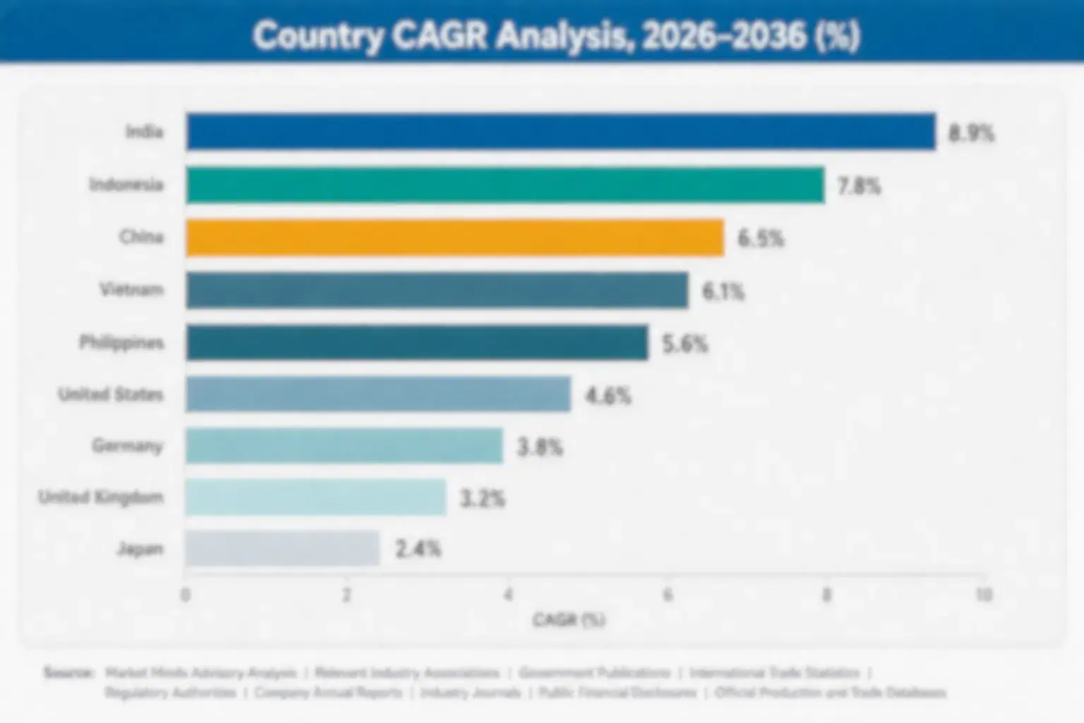
integrated-cmos-tri-gate-transistor-market-country-cagr-analysis-1788851837777

Monetizing Allocation, Packaging, and Co-Design

Foundries are finding that the largest incremental margin sits outside the base wafer price, in priority allocation premiums, advanced packaging services, and automotive qualification co-design fees layered onto capacity that customers across nearly every major industry vertical are already competing intensely to secure across this entire decade and well beyond it into the next.

Charging Premium Pricing for Priority Node Allocation

Given persistent demand outstripping supply at the most advanced tri-gate nodes, foundries are charging premium pricing for guaranteed priority allocation rather than serving all customers on a strict first-come basis regardless of contract size or relationship history with the foundry itself over time. Customers willing to pay allocation premiums secure wafer capacity months ahead of standard-queue customers, and foundries report allocation premiums adding roughly 14 percent to effective realized pricing for customers who opt into priority contracts. This approach also gives foundries better demand visibility for long-term capacity planning purposes.
Market Impact: Adds roughly a 14 percent priority allocation premium

Bundling Advanced Packaging Services With Wafer Fabrication

Foundries are increasingly bundling advanced packaging, including chiplet integration and high-bandwidth memory stacking, directly with wafer fabrication rather than leaving customers to source packaging separately from a third party assembly house elsewhere in the much broader global supply chain today. This bundled offering captures packaging margin that previously went to standalone assembly and test houses, and foundries report packaging-attached revenue reaching roughly 26 percent of total customer contract value for advanced-node orders. Customers also benefit from a single accountable vendor relationship across the entire manufacturing process from start to finish.
Market Impact: Captures roughly a 26 percent packaging-attached revenue share

Offering Automotive Chip Qualification Co-Design Services

Foundries are packaging automotive-grade qualification engineering as a premium co-design service for chip designers entering the automotive market for the first time without in-house automotive reliability expertise of their own to draw upon internally at any real meaningful scale. This service captures high-margin engineering fees separate from eventual wafer production revenue, and foundries offering automotive qualification services report engagement fees averaging roughly 25 million dollars per customer programme before volume production even begins in earnest. The relationship also typically locks the customer into multi-year production commitments once qualification is complete.
Market Impact: Captures roughly 25 million dollars in engagement fees

Expanding Design-For-Manufacturing Consulting and Engineering Services

Foundries are offering design-for-manufacturing consulting that helps fabless customers optimize chip layouts specifically for a given process node before committing to expensive mask sets, reducing the risk of costly re-spins after initial fabrication runs. This consulting revenue is captured well before the customer places a production order, giving foundries earlier visibility into upcoming demand across the pipeline, and foundries offering the service report re-spin rates dropping by roughly 30 percent among customers who use the consulting service compared with those customers who do not use it at all in their design flow.
Market Impact: Reduces customer chip re-spin rates by 30 percent

Who Controls the Margin Pool

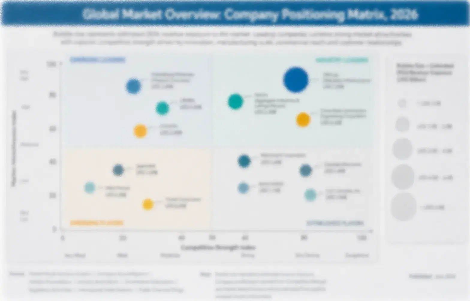
At an estimated 62 percent combined share, the top five vendors hold a dominant lead over a long tail of specialty and mature-node foundries, and the gap between the leading suppliers and the next tier is widening as gate-all-around transition costs become a harder capital investment for smaller challengers to replicate quickly without outside government support of some kind.
Current competitive activity centers on three fronts: racing to develop gate-all-around transistor capability ahead of rivals rather than extending tri-gate life indefinitely, forming government-backed fabrication partnerships to secure subsidized construction costs for new advanced-node facilities across multiple countries, and offering automotive and packaging co-design services to defend customer relationships against fabless customers considering alternative foundries.

Emerging pressure is coming from national champion foundries backed by government industrial policy, undercutting established incumbents on price for customers willing to accept somewhat less advanced process technology in exchange for lower cost. Rankings are most likely to shift wherever a challenger secures scarce extreme ultraviolet lithography equipment allocation before an incumbent does, since equipment access has become as decisive a competitive advantage as process technology itself in this constrained market.
integrated-cmos-tri-gate-transistor-market-company-positioning-matrix-1788851838068

Competitive Moat and Risk Dimensions

TSMC

Moat: Leading-Edge Process Node Scale

TSMC's scale and yield leadership at the most advanced process nodes gives it a customer base that includes nearly every major fabless chip designer worldwide, and switching to a competing foundry requires redesigning chips against a different process design kit that few competitors can match in maturity.
TSMC

Risk: Geographic Concentration Risk in Taiwan

TSMC's manufacturing base remains heavily concentrated in Taiwan despite recent overseas expansion, and escalating geopolitical tension around the island represents a systemic risk that no amount of individual customer diversification can fully offset for the entire broader global chip supply chain over the coming years.
INTEL

Moat: Integrated Design and Manufacturing Model

Intel's combined chip design and manufacturing model gives it tighter internal coordination between architecture and process technology than pure foundries offer external customers, and its domestic United States manufacturing base appeals strongly to customers and governments prioritizing supply chain diversification well away from East Asia.
INTEL

Risk: Process Node Leadership Recovery Uncertainty

Intel has trailed TSMC and Samsung on process node leadership for several consecutive generations, and its foundry business must prove it can reliably match leading-edge yields before major external customers commit meaningful production volume rather than treating Intel as a secondary or backup source only.

Players Tracked

Prominent Players

TSMC
Intel
Samsung Electronics
GlobalFoundries
United Microelectronics Corporation

Other Key Players

SMIC
Micron Technology
SK Hynix
Texas Instruments
STMicroelectronics
NXP Semiconductors
Infineon Technologies
Renesas Electronics
Tower Semiconductor
Vanguard International Semiconductor
PSMC
ASE Technology Holding
Nexchip Semiconductor
Huahong Semiconductor
X-FAB Silicon Foundries

Recent Developments

SEPTEMBER 2025

TSMC Announces Volume Production Ramp for Gate-All-Around Node

TSMC announced volume production ramp for its next-generation gate-all-around transistor process node, extending its process technology roadmap considerably ahead of several pending customer qualification cycles scheduled for the entire coming year across multiple leading fabless chip design customers based worldwide and well beyond that point.
Signal: Extends TSMC's process technology leadership considerably ahead of several major customer qualification cycles due next year
JANUARY 2026

Intel Acquires Advanced Chiplet Packaging Technology Startup

Intel acquired an advanced packaging technology startup specializing in chiplet integration, adding capability that Intel had previously licensed from a third-party partner under a less favorable commercial arrangement that limited roadmap flexibility. The acquisition brings packaging technology fully in-house ahead of several foundry customer contracts scheduled for the coming year.
Signal: Brings packaging technology fully in-house at Intel, considerably reducing dependence on costlier third-party licensing arrangements entirely
MAY 2025

GlobalFoundries Forms Joint Venture for Government-Backed Fabrication Facility

GlobalFoundries formed a joint venture with a national government to build a new advanced-node fabrication facility supporting domestic automotive and defense chip supply, combining GlobalFoundries' process technology with substantial government construction subsidies and firm long-term offtake commitments from multiple domestic customers nationwide and well beyond.
Signal: Opens a new government-backed fabrication facility for GlobalFoundries supporting long-term domestic chip supply needs ahead of schedule

Lithography, Wafer, and Materials Costs

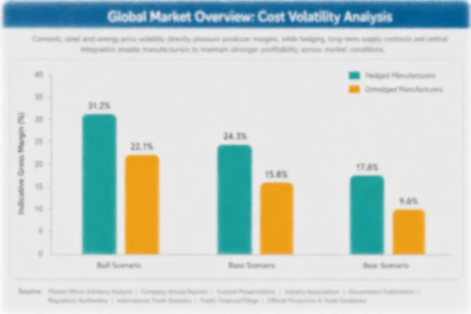
Extreme ultraviolet lithography equipment depreciation and specialty silicon wafer costs together account for roughly 42 to 50 percent of vendor cost of goods sold for advanced tri-gate process nodes, with lithography equipment sourced almost entirely from a single dominant supplier whose pricing terms foundries have limited leverage to negotiate. Specialty process gases and photoresist chemicals add the next largest cost line.
The 2024 to 2025 rise in specialty gas and photoresist pricing, driven by demand from expanding advanced-node capacity competing for the same limited chemical supply, pushed materials costs up meaningfully according to company investor disclosures. Foundries with long-term materials supply agreements absorbed the increase more gradually, while smaller vendors paying closer to spot pricing saw margin compression on fixed-price customer contracts signed before the increase.

The competitive disadvantage falls hardest on smaller foundries that lack the purchasing scale to negotiate reserved lithography equipment and specialty materials agreements, forcing them to compete for limited equipment deliveries against larger rivals with standing supplier relationships. Foundries with long-term equipment supply contracts can plan capacity expansion more aggressively, widening the gap between scaled incumbents and smaller regional foundries over successive process node generations.
integrated-cmos-tri-gate-transistor-market-cost-volatility-analysis-1788851838415

Multi-Year Lithography Equipment Supply Agreements

Leading foundries are locking in multi-year lithography equipment and specialty materials supply agreements directly with manufacturers to smooth exposure to price spikes and delivery delays affecting the broader global semiconductor equipment industry as a whole. These agreements typically trade a modest capacity commitment premium for delivery certainty that lets foundries plan capacity expansion confidently.

Standardizing Process Recipes Across Product Lines

Foundries are designing process recipes that share common materials and equipment configurations across multiple customer products rather than custom-engineering each recipe separately, reducing the variety of specialty chemicals purchased and increasing per-material order volume with suppliers considerably each year. This standardization improves negotiating position on unit pricing even without formal reserved-capacity agreements in place.

Portfolio Architecture for Margin Defence

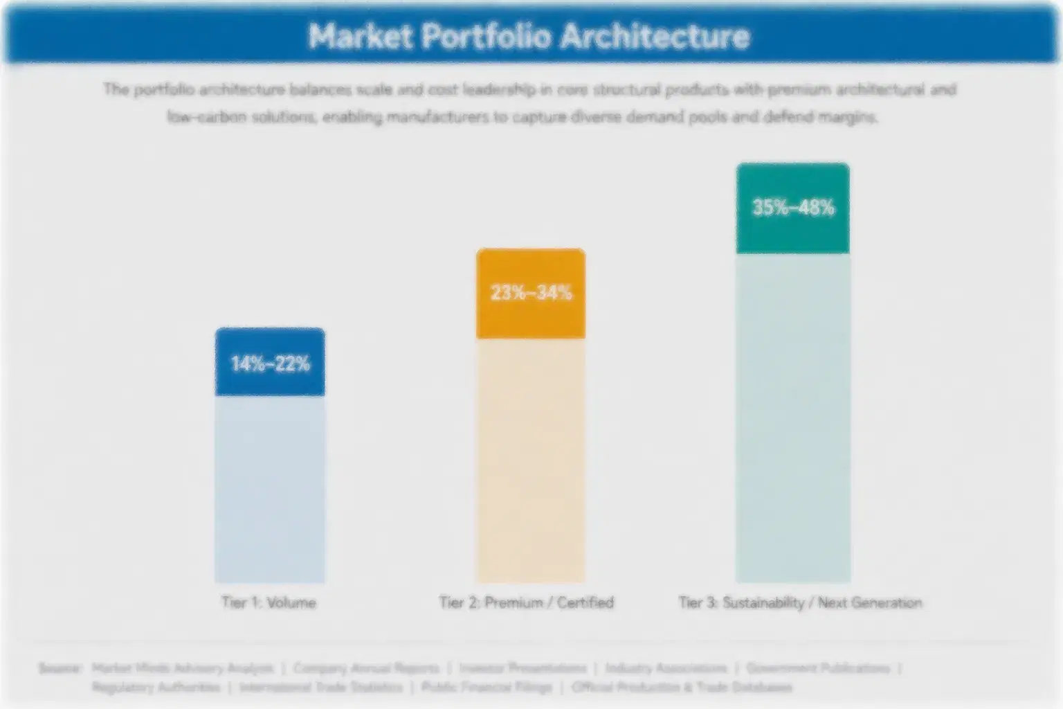
Portfolio economics split cleanly along three tiers: commodity mature-node wafers sold mostly on unit price, certified mainstream advanced-node capacity sold on yield and reliability assurance, and next-generation leading-edge and gate-all-around capacity sold on premium allocation terms. Gross margin widens sharply moving up this ladder, since leading-edge capacity commands pricing power that mature nodes never achieve given how few foundries can supply it.
The volume tier still generates the largest wafer shipment count by far, dominated by mature-node capacity sold into automotive, industrial, and commodity electronics customers who treat competing foundries as largely interchangeable on price. Premium tiers instead compete on yield consistency and process design kit maturity, and AI and high-performance computing customers there pay materially more for guaranteed leading-edge access rather than for raw wafer count alone.

High-value margin pools concentrate almost entirely in leading-edge and gate-all-around capacity contracts, where allocation premiums and packaging bundling command pricing power well above anything the mature-node tier can support today. Foundries positioned purely on mature-node capacity increasingly find themselves squeezed toward the bottom of the portfolio as the highest-margin customers pay for leading-edge access over raw wafer volume.

Mature-node wafer capacity sold into automotive, industrial, and commodity electronics customers, priced almost entirely on unit cost with thin differentiation between competing foundries and very limited room for margin expansion.
Gross Margin

Certified mainstream advanced-node capacity with proven yield and process design kit maturity, sold into customers that require documented reliability before any large production contract is ever awarded and subsequently renewed.
Gross Margin

Leading-edge and gate-all-around capacity priced on premium allocation terms rather than commodity wafer cost, with margin scaling alongside customer priority tier, packaging bundling, and the overall size of the contract.
Gross Margin
integrated-cmos-tri-gate-transistor-market-portfolio-architecture-1788851838735

High-value Sub-segments and Strategic Watch-out

Leading-Edge AI Accelerator Capacity

Leading-edge AI accelerator capacity, where premium allocation pricing justifies high margin and demand is accelerating well ahead of most other segments as hyperscalers scale training infrastructure at an unprecedented pace worldwide this year, pulling forward demand considerably from customers that had planned much slower ramps.

Automotive-Qualified Advanced-Node Capacity

Automotive-qualified advanced-node capacity, where large multi-year production commitments and qualification fees deliver reliable margin even as unit growth moderates from earlier peak years in consumer electronics markets overall and worldwide, leaving a dependable base of renewal revenue for foundries that qualified early in the cycle.

Mature-Node Wafer Capacity

Mature-node wafer capacity, the largest unit-volume segment overall but one facing continual price compression from commoditized capacity and a rising number of national-champion regional foundries entering the entire global market each year with broadly comparable capabilities, features, pricing, and progressively much thinner incumbent margin overall.

Standalone Planar Transistor Chips

Standalone planar transistor chips sold without tri-gate architecture, which face mounting displacement pressure as customers migrate toward tri-gate and gate-all-around designs instead, risking a lasting decline in demand for older chip technology across most industries, geographies, and end markets worldwide today, tomorrow, and well beyond.

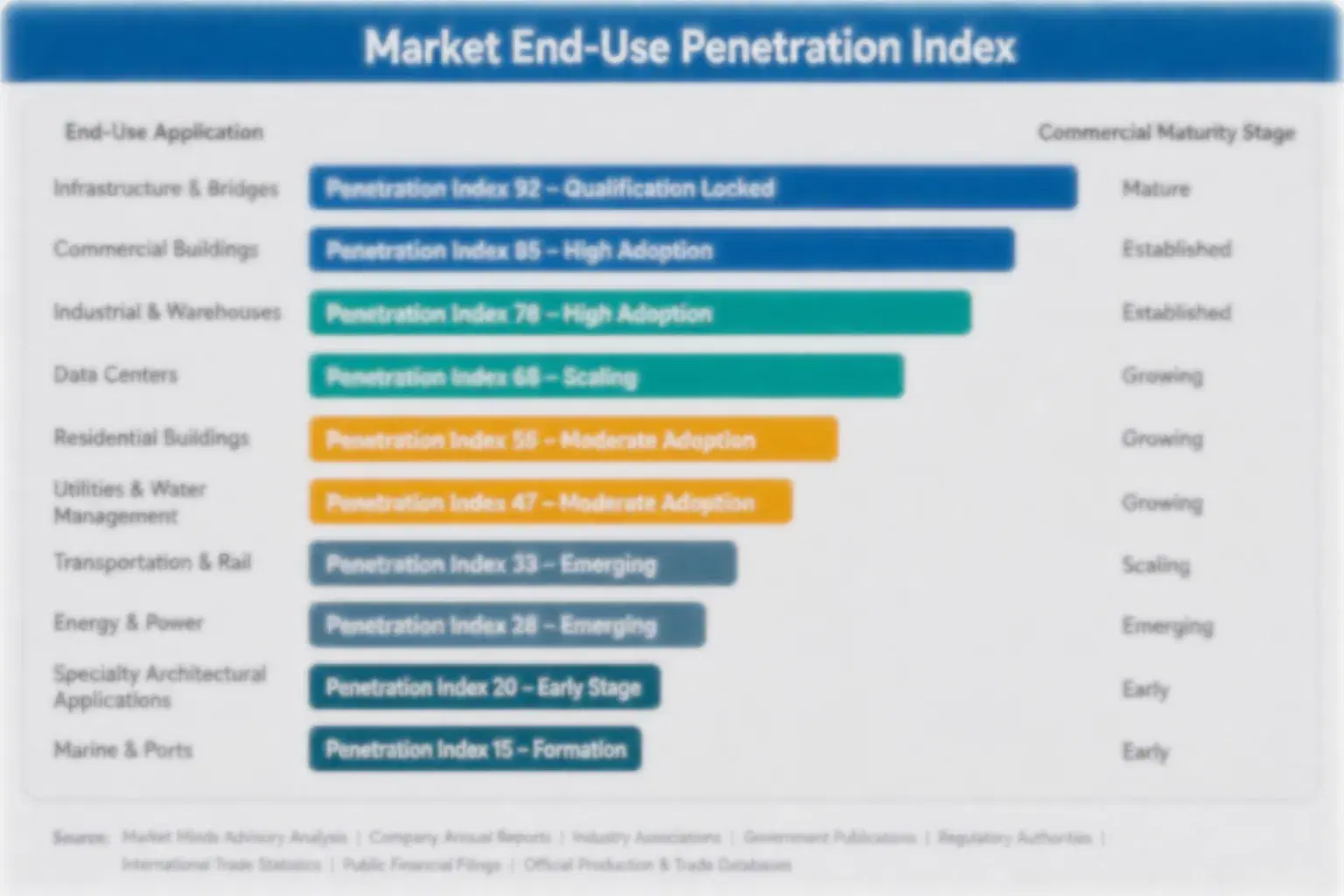
Why Process Node Choice Locks Loyalty

Foundry relationships behave like annuities once a chip design is taped out against a specific process design kit, since migrating to a competing foundry requires re-taping the entire chip design from scratch rather than simply switching a supplier. Customers renew rather than switch, and renewal pricing typically holds firm as process node capability deepens with each successive generation.
Stickiness varies by vertical: automotive and industrial customers renew at very high rates because switching risks a lengthy requalification process that regulators and safety standards require before any production change, while consumer electronics customers switch more freely since their qualification requirements are lighter and switching costs are correspondingly lower still. AI accelerator customers sit between the two, renewing steadily but occasionally dual-sourcing across foundries to manage capacity risk.

A generational shift in buyer profile is underway as chip architects and supply chain risk officers, rather than procurement teams focused purely on unit cost, increasingly own the foundry selection decision, weighting geographic diversification and packaging capability over raw wafer price alone. That shift favors foundries who can demonstrate resilient, geographically diversified capacity over those competing on price alone.
integrated-cmos-tri-gate-transistor-market-end-use-penetration-index-1788851839002

Where MMA Sees Durable Advantage

These are among the four positions where our research anticipates prominent divergence between winners and laggards over the coming forecast period. Each is grounded in the demand model, the regulatory perimeter, and the announced capacity pipeline.
01 / GATE-ALL-AROUND TRANSITION TIMING

Track gate-all-around readiness as the key foundry differentiator

Buyers evaluating foundry partners should weight gate-all-around transition readiness at least as heavily as current tri-gate yield performance, since the foundries best positioned for the next architecture generation will capture the largest share of future advanced-node contracts across every major customer segment. Foundries that can demonstrate a credible gate-all-around roadmap are winning long-term commitments well before competitors still extending tri-gate life indefinitely without a clear transition plan. This dynamic will intensify as the physical limits of tri-gate scaling become more apparent industry-wide.
02 / PRIORITY ALLOCATION INVESTMENT

Secure priority capacity allocation ahead of the next demand surge

Chip designers dependent on leading-edge capacity should negotiate priority allocation agreements now rather than waiting for the next AI demand surge to compress available capacity even further than it already has today. Foundries are already charging meaningful premiums for guaranteed allocation, and that premium will likely rise as AI accelerator demand continues absorbing a growing share of leading-edge output across the industry. Locking in allocation early protects against being pushed to the back of an increasingly long capacity queue for years to come.
03 / TAIWAN CONCENTRATION RISK

Treat Taiwan concentration as a material planning risk

Taiwan's dominance in advanced tri-gate manufacturing makes it the single point of failure for nearly every leading chip supply chain worldwide, regardless of which country designs the underlying chip architecture or headquarters the fabless firm involved directly. Buyers and investors should treat geopolitical tension around the island as a material supply risk requiring active contingency planning rather than a distant, abstract concern worth ignoring entirely. Foundries diversifying into alternative manufacturing geographies deserve a meaningful valuation premium for that added resilience.
04 / AUTOMOTIVE QUALIFICATION REVENUE

Build automotive qualification services ahead of rising demand

Foundries and chip designers alike underestimate how much long-term value sits in automotive qualification services rather than in the initial wafer sale itself, since automotive relationships compound meaningfully over multi-year vehicle production cycles that span a decade or more. Building automotive qualification capability early, rather than treating it as a niche afterthought, measurably improves lifetime contract value and positions foundries well ahead of rivals still focused primarily on consumer electronics customers. That discipline is becoming a genuine differentiator between competing foundries.

Engagement Snapshot From the Field

A live engagement with an industry participant carrying material or product regulatory and market exposure ahead of a defining policy shift, showing how our research translates into a defensible multi-year portfolio strategy.
MARKET MINDS ADVISORY · CLIENT ENGAGEMENT SUMMARY
Integrated CMOS Tri-gate Transistor Producer Strategic Portfolio Review and Transition Roadmap 2026·Investment Scenario on Integrated CMOS Tri-gate Transistor Exposure Evaluation 2025-26
CLIENT PROFILE
The client is a leading fabless AI accelerator designer whose chips power inference workloads for major cloud providers and enterprise customers worldwide across dozens of data centers. Facing persistent capacity shortages from its sole foundry partner, the company needed a dual-sourcing strategy to reduce dependence on a single manufacturer without disrupting committed customer delivery timelines.
STRATEGIC CHALLENGE
The company's chip designs were optimized entirely around one foundry's process design kit, and internal engineering teams estimated that porting even a subset of designs to a second foundry would require substantial redesign work and a lengthy requalification process. Leadership needed a phased dual-sourcing roadmap that would not disrupt existing customer commitments.
MMA APPROACH
MMA assessed three alternative foundries against a common evaluation framework covering process design kit compatibility, capacity availability, and total cost of ownership across a full five-year horizon. The engagement included a phased design-porting roadmap and a foundry negotiation playbook designed to secure long-term capacity commitments ahead of peak demand periods.
KEY FINDINGS
  1. Two of the three alternative foundries lacked process design kit compatibility mature enough to fully support the company's most advanced chip designs.
  2. Porting a pilot chip design to the selected second foundry took approximately 35 percent longer than initially budgeted (client-reported, unverified by MMA).
  3. The selected foundry offered multi-year capacity guarantees that meaningfully reduced projected shortage risk for the company's largest ongoing customer commitments overall today.
  4. Customer delivery timelines held steady throughout the entire dual-sourcing transition period with no measurable disruption ever actually reported (client-reported, unverified by MMA).
CLIENT PROFILE
The client is a leading fabless AI accelerator designer whose chips power inference workloads for major cloud providers and enterprise customers worldwide across dozens of data centers. Facing persistent capacity shortages from its sole foundry partner, the company needed a dual-sourcing strategy to reduce dependence on a single manufacturer without disrupting committed customer delivery timelines.
STRATEGIC CHALLENGE
The company's chip designs were optimized entirely around one foundry's process design kit, and internal engineering teams estimated that porting even a subset of designs to a second foundry would require substantial redesign work and a lengthy requalification process. Leadership needed a phased dual-sourcing roadmap that would not disrupt existing customer commitments.
MMA APPROACH
MMA assessed three alternative foundries against a common evaluation framework covering process design kit compatibility, capacity availability, and total cost of ownership across a full five-year horizon. The engagement included a phased design-porting roadmap and a foundry negotiation playbook designed to secure long-term capacity commitments ahead of peak demand periods.
KEY FINDINGS
  1. Two of the three alternative foundries lacked process design kit compatibility mature enough to fully support the company's most advanced chip designs.
  2. Porting a pilot chip design to the selected second foundry took approximately 35 percent longer than initially budgeted (client-reported, unverified by MMA).
  3. The selected foundry offered multi-year capacity guarantees that meaningfully reduced projected shortage risk for the company's largest ongoing customer commitments overall today.
  4. Customer delivery timelines held steady throughout the entire dual-sourcing transition period with no measurable disruption ever actually reported (client-reported, unverified by MMA).
RECOMMENDED STRATEGY
Phase 1: Phase 1 (Months 1-4): Port a pilot chip design very carefully onto the second foundry's own selected process design kit. Phase 2: Phase 2 (Months 5-10): Qualify the pilot design fully and begin limited production at the newly selected second foundry partner. Phase 3: Phase 3 (Months 11-16): Scale dual-sourcing gradually across additional chip designs and all existing customer commitments made nationwide today and beyond.
OUTCOME
The company successfully diversified a meaningful share of its production capacity across two foundries without disrupting existing customer commitments. Supply reliability improved measurably, and the company reported reduced exposure to single-foundry shortage risk within the first year of the dual-sourcing programme (client-reported, unverified by MMA), though full design-portfolio parity across both foundries remains in progress.

Frequently Asked Questions

Foundational context covering the market sizes, CAGR, scope, country, region and competition that inform every finding below. This section is provided to cover basics and most often pre-purchase conversations, answered from the MMA Primary Research Dataset.

What is the current size of the Integrated CMOS Tri-gate Transistor Market?

The integrated CMOS tri-gate transistor market is valued at approximately $14.2 billion in 2025. This figure covers semiconductor chips fabricated using three-dimensional tri-gate transistor architecture worldwide.

How large will the Integrated CMOS Tri-gate Transistor Market be by 2036?

MMA projects the market will reach approximately $43.0 billion by 2036. That represents nearly a threefold expansion from the 2026 base value of $15.7 billion.

What is the CAGR for the Integrated CMOS Tri-gate Transistor Market 2026 to 2036?

The market is forecast to grow at a 10.6 percent compound annual rate between 2026 and 2036. Bull and bear scenarios range from 9.3 to 11.9 percent.

Which segment is growing fastest?

AI accelerator and GPU chips are the fastest-growing segment, expanding at an estimated 18.0 percent CAGR through 2036. That is roughly 1.70 times the overall market growth rate.

Who are the major companies in the Integrated CMOS Tri-gate Transistor Market?

TSMC, Intel, Samsung Electronics, GlobalFoundries, and United Microelectronics Corporation lead the market. Together they hold an estimated 62 percent combined share on a revenue basis.

Which country is growing fastest?

Taiwan is the fastest-growing country, expanding at an estimated 15.2 percent CAGR through 2036. Growth is driven by continued leadership in advanced wafer fabrication and packaging capacity.

Report Segmentation Architecture

The full report scope spans multiple orthogonal segmentation dimensions, with cross-tabulated demand data provided for each dimension pair. Coverage extends further to regional breakdowns, trend trajectories, and the competitive detail needed to support segment-level decision-making.

By Primary Market Dimension

  • High-Performance Computing and Data Center Processors
  • Mobile and Consumer Electronics Processors
  • Automotive and Industrial Semiconductors
  • AI Accelerator and GPU Chips
  • Networking and Communications Chips
  • IoT and Edge Device Chips

By End-Use Industry

  • Cloud and Data Center
  • Automotive
  • Consumer Electronics
  • Telecommunications
  • Industrial and Manufacturing

By Commercial Dimension

  • Merchant Foundry Services
  • Integrated Device Manufacturing
  • Design and IP Licensing
  • Advanced Packaging Services

By Region

  • North America
  • Western Europe
  • East Asia
  • South Asia and Pacific
  • Latin America
  • Middle East and Africa
  • Eastern Europe

Scope, Methodology, and Coverage

Every figure in this report is reproducible from documented input assumptions. The scope below maps the historical period, the forecast horizon, the segmentation dimensions, and the countries covered, alongside the underlying primary and qualitative methodology.
Historical Period
2020 to 2025
Forecast Period
2026 to 2036
Base Year
2025 (USD billions; MMA Primary Research Dataset, September 2026)
Market Definition
The integrated CMOS tri-gate transistor market covers semiconductor chips fabricated using three-dimensional tri-gate, or FinFET, transistor architecture across all process nodes and end-use applications. It excludes planar transistor chips fabricated on older process technology and next-generation gate-all-around transistor chips not yet in volume commercial production.
Quantitative Units
USD billions (current prices); wafer shipment volumes where applicable
Segmentation Dimensions
End-Use Application; End-Use Industry; Commercial Dimension; By Region
Regions Covered
North America, Western Europe, East Asia, South Asia and Pacific, Latin America, Middle East and Africa, Eastern Europe
Countries Covered
USA, China, Germany, France, UK, Japan, South Korea, India, Australia, Canada, Brazil, Mexico, Indonesia, Vietnam, Thailand, Malaysia, UAE, Saudi Arabia, South Africa, Nigeria, Turkey, Poland, Netherlands, Italy, Spain, Sweden, Switzerland, Argentina, Colombia, Singapore, and additional markets relevant to this sector
Key Companies Profiled
TSMC, Intel, Samsung Electronics, GlobalFoundries, United Microelectronics Corporation, SMIC, Micron Technology, SK Hynix, Texas Instruments, STMicroelectronics, NXP Semiconductors, Infineon Technologies, Renesas Electronics, Tower Semiconductor, Vanguard International Semiconductor, PSMC, ASE Technology Holding, Nexchip Semiconductor, Huahong Semiconductor, X-FAB Silicon Foundries
Quantitative Methodology
Primary survey, n=3,800 respondents, Q4 2025, six countries; demand-side model with trade association cross-validation
Qualitative Methodology
47 expert interviews, Q4 2025; applied to validate demand model assumptions, identify emerging dynamics, and assess competitive positioning
Report Format
PDF and XLSX data workbook (Word format preview document)
Publisher
Market Minds Advisory
Report Code
MMA-2026-TEC-667
Published
September 2026
Contact
sales@marketmindsadvisory.com | www.marketmindsadvisory.com

Purchase the full Integrated CMOS Tri-gate Transistor Market Report (2026 to 2036).

This report provides a ten-year quantitative sizing and forecast model for the integrated CMOS tri-gate transistor market, covering advanced-node and mature-node wafer production across all seven global regions. It includes detailed segmentation by end-use application, competitive benchmarking of the top twenty vendors, and a proprietary MMA Primary Research dataset drawn from expert interviews and a large-scale quantitative survey. Buyers receive regional deep-dives, vendor moat and risk assessments, and forward-looking scenario modeling calibrated against historical adoption patterns. An anonymized case study and a full revenue-lever breakdown round out the deliverable for teams building foundry strategy or supply chain diversification roadmaps.
Ten-year quantitative market sizing and forecast model
Segmentation by end-use application and process node
Vendor moat and risk assessment for top players
Regional deep-dives across all seven global regions
Primary survey and expert interview dataset access
Revenue lever and portfolio margin benchmarking analysis

Built For The People Who Decide

From boardroom strategy to bench-side execution, this report is read cover-to-cover by leaders shaping the next decade of their industry, turning demand scenarios, market dynamics and valuation benchmarks into decisions.
CXOs/ Presidents/ VPs/ Managers
M&A and Corporate Development
Strategy Teams and R&D Heads
Procurement and Product Directors
Regulatory and Compliance Leaders
Investor Relations and Equity Analysts