Market Minds Advisory
GaN Substrate Market

GaN Substrate Market: GaN Substrate Market: Substrate Constructions, Defect Economics and Crystal Growth Routes 2026 to 2036

Almost every gallium nitride device on earth is grown on something that is not gallium nitride. The substrate that would fix that problem costs a hundred times more than the alternative.

Lead Analyst

Published

September 2026

Make Smarter Decisions with Customized Research Insights

Request a free sample report and evaluate market opportunities, growth trends, and competitive dynamics relevant to your business needs.

2025 MARKET VALUE$0.9BMarket Size 2025
2036 FORECAST VALUE$3.7BBase Case , 2026 to 2036
CAGR 2026 TO 203613.8 %Bull 15.2% / Bear 12.5%
INCREMENTAL OPPORTUNITY$2.7BNet 10- year value creation
EXPANSION MULTIPLE3.65x2036 value over 2026 base
Strategic Levers
M&A Pipeline
Regional Outlook
Country Rankings
Competitive Intelligence
Segmental Deep-dive
Call-Us : 91 93563 13602

Executive Snapshot and Market Trajectory.

Gallium nitride has a substrate problem nobody has solved. Devices are grown on silicon, sapphire or silicon carbide because freestanding gallium nitride costs about a hundred times more, and every one of those devices carries a lattice mismatch and a defect density that silicon manufacturing would never accept.
The market reaches USD 1.02 billion in 2026 and USD 3.72 billion by 2036, a 3.65 times expansion at 13.8%. Ammonothermal bulk substrates grow at 20.7%, half again the market rate of 13.8%, because growing a crystal in a pressure vessel is the one route that could close the price gap. East Asia holds 56% of shipment area, and China alone grows at 18.9%. The growth rate is glacially slow, which is the whole difficulty.
Five suppliers hold 68% of shipment area, concentrated by crystal growth capability rather than by capacity. Japanese chemical companies including Sumitomo and Mitsubishi Chemical own most of the bulk substrate technology. Coherent and Kyocera compete on epitaxial wafers. Chinese producers hold enormous volume in sapphire and silicon based epi, and are pushing hard into bulk growth with state funding behind them. Nobody there is short of patience.
Market Definition
This report covers substrates on which gallium nitride devices are grown: gallium nitride on silicon, on silicon carbide and on sapphire epitaxial wafers, and freestanding bulk gallium nitride substrates grown by hydride vapour phase epitaxy, ammonothermal and sodium flux methods. It excludes finished gallium nitride devices, silicon carbide substrates for silicon carbide devices, bare sapphire and silicon wafers sold as commodity substrates, and epitaxial deposition equipment.
Base Year Value
$0.9B in 2025 (MMA Primary Research Dataset, September 2026)
Forecast Period
2026 to 2036, eleven discrete annual values
CAGR
13.8% base case. Bull 15.2%. Bear 12.5%.
Fastest Growth Segment
Ammonothermal Bulk GaN Substrates: 20.7% CAGR
Fastest Growth Country
China: 18.9% CAGR
Fastest Growth Region
South Asia and Pacific: 15.8% CAGR
Largest Region
East Asia: 56% of 2025 global value
Market Leaders
Sumitomo Chemical, Mitsubishi Chemical Group, Sumitomo Electric Industries, Coherent and Kyocera lead on substrate and epitaxial wafer shipment area. Source: MMA Analysis.
Primary Survey
n=3,800 procurement and R&D decision-makers, Q4 2025, six countries
Methodology
Demand-side build-up, cross-validated against public data, 47 expert interviews

GaN Substrate Market Forecast Scenarios

gan-substrate-market-size-forecast-scenario-1789986980791
Between 2020 and 2025 the category compounded at 12.6%, and almost all of that came from power electronics rather than from lighting. Gallium nitride chargers moved from a novelty to a mainstream product, which pulled enormous volume through gallium nitride on silicon epitaxy. Bulk substrate volume barely moved, because the price gap against foreign substrates did not close at all.
The base case holds 13.8% on three mechanisms. Power conversion keeps pulling gallium nitride on silicon epitaxy at volume, since a charger, a data centre supply and a solar inverter all want a faster switch. Radio frequency demand for defence radar and telecommunications infrastructure sustains gallium nitride on silicon carbide at high value and modest area. And laser diodes for displays, materials processing and automotive lighting need low defect freestanding material that nothing else can supply.
The bull case at 15.2% assumes ammonothermal growth reaches commercial throughput and 4 inch freestanding substrates arrive at a price vertical power device makers will pay. The bear case at 12.5% is Chinese epitaxial capacity expanding faster than device demand, which would collapse pricing on gallium nitride on silicon and drag the whole average down with it.

The Substrate Gallium Nitride Never Had

Silicon devices are built on silicon. Gallium nitride devices are mostly built on something else, because a freestanding gallium nitride substrate costs roughly a hundred times what a silicon or sapphire wafer of comparable diameter costs. The consequence is a lattice mismatch at the interface and a defect density around a billion per square centimetre, which is a number that would end a career in silicon manufacturing.
TOP FIVE CONCENTRATION68%Concentrated by crystal growth capability rather than by capacity
FREESTANDING SUBSTRATE DIAMETER2 inchesStandard commercial size for bulk gallium nitride today
EPITAXIAL DEFECT DENSITY1 billion per cm2Typical for gallium nitride grown on silicon wafers
FREESTANDING PRICE PREMIUM100xAgainst a foreign substrate of comparable usable diameter
AMMONOTHERMAL GROWTH RATE30 microns dailyCrystal thickness added in a single pressure vessel run
EPITAXIAL WAFER YIELD72%Usable die area after edge exclusion and defect mapping
For most applications that defect density is survivable. An LED still lights, and a lateral power transistor at 650 volts still switches acceptably. For a laser diode, or a vertical device holding off higher voltage, it decides whether the part works at all. That split is why the market has two halves that behave nothing like each other: enormous cheap epitaxial area, and small expensive freestanding wafers.
Diameter is the other constraint and it is the more embarrassing one. Silicon runs at 300 millimetres. Commercial freestanding gallium nitride is still at 2 inches and struggling toward 4. Every doubling of diameter roughly quarters the substrate cost per die, so the whole economics of vertical gallium nitride devices waits on a crystal growth problem that has resisted thirty years of effort.
"The gallium nitride industry spent twenty years getting very good at growing crystals on the wrong material. That was the pragmatic choice and it worked. It also means the moment somebody grows a cheap 4 inch bulk wafer, a great deal of accumulated expertise becomes worth considerably less."
Principal, Compound Semiconductor Materials Practice · MMA Chemicals and Materials Practice · September 2026

Market Trends

Ammonothermal Growth Is The Only Credible Cost Route

Every other method of growing bulk gallium nitride is a deposition process, which means growing a crystal one layer at a time on a seed and inheriting whatever went wrong underneath. Ammonothermal growth works like a chemical process instead: gallium nitride dissolves in supercritical ammonia at high pressure and recrystallises on a seed, producing far lower defect density and, in principle, many wafers per run. The problem is throughput. Growth adds roughly 30 microns a day, so a usable boule takes months and the pressure vessels are genuinely exotic equipment.
Market Impact: Radar epitaxy compounds at 12.9%
Power Conversion Pulled Epitaxial Volume Past Lighting

Gallium nitride began as a lighting material and the epitaxial capacity built for LEDs was enormous. Power electronics has now taken over as the volume driver, because a wide bandgap switch runs at far higher frequency and shrinks the magnetics around it, which is why a 65 watt charger fits in a pocket. That demand runs almost entirely on gallium nitride grown on silicon, since a lateral device at 650 volts tolerates the defect density and silicon wafers are cheap and available in large diameters. Lighting demand has been flat for years now.
Market Impact: Defects fall 4 orders of magnitude

Market Opportunities and Growth Drivers

Defence Radar Sustains High Value Silicon Carbide Epitaxy

Gallium nitride grown on silicon carbide is the standard material for active electronically scanned array radar, because silicon carbide conducts heat far better than silicon or sapphire and a radar transmit module runs hot. Defence procurement across the United States, Europe, Japan and Korea has expanded steadily, and telecommunications base station amplifiers use the same material. The segment compounds at 12.9% on modest wafer area at very high value per square inch, and qualification cycles running several years make the incumbent position unusually secure. Nobody displaces a qualified radar supplier quickly.
Market Impact: Substrates stuck at 2 inches

Laser Diodes Need Material Nothing Else Supplies

A laser diode cannot be built on a substrate carrying a billion defects per square centimetre, because each defect is a place where the device fails under optical power density. Freestanding gallium nitride gets defect density down by four orders of magnitude, and that is why every blue and green laser diode in projection displays, materials processing and automotive lighting is built on bulk material. The application is small in area and enormous in value per wafer, and it is the only demand keeping bulk substrate producers commercially viable at present.
Market Impact: Sapphire epitaxy pricing fell 30%

Market Restraints and Challenges

Diameter Has Barely Moved In Thirty Years

Commercial freestanding gallium nitride is still supplied at 2 inches while silicon runs at 300 millimetres, and every doubling of diameter roughly quarters the substrate cost per die. The root cause is that gallium nitride does not melt at accessible pressure, so the Czochralski pulling that made large silicon boules cheap is simply unavailable and every route is slower and smaller. Commercially this keeps vertical device economics out of reach. Mitigation runs through ammonothermal scaling and through engineered composite substrates that mimic bulk properties on a larger carrier. Neither route is close to volume yet.
Market Impact: Growth adds 30 microns daily

Chinese Epitaxial Capacity Threatens Wafer Pricing

Chinese producers built vast gallium nitride on sapphire capacity for the LED industry and have been converting it toward power and radio frequency epitaxy with provincial and national support behind them. The root cause is that epitaxial deposition capacity is capital equipment rather than accumulated crystal growth knowledge, so it can be bought and installed far faster than expertise can be developed. Commercially this compresses pricing across the volume half of the market. Mitigation runs through moving into bulk substrates and engineered wafers, where the barrier is knowledge rather than equipment.
Market Impact: Chargers at 65 watts drive volume
2 additional market trends, 4 additional growth drivers, and 3 additional restraints and challenges are covered in the full report. Contact sales@marketmindsadvisory.com to access the complete intelligence.

Segment CAGR and Growth Architecture

Segmentation follows substrate construction, since what a device is grown on determines its defect density, cost and application reach. Six classes cover the market: ammonothermal bulk substrates, gallium nitride on silicon epitaxial wafers, hydride vapour phase epitaxy freestanding substrates, gallium nitride on silicon carbide, sodium flux and other bulk routes, and gallium nitride on sapphire. Application is a separate dimension.
gan-substrate-market-market-share-analysis-1789986981376

Ammonothermal Bulk GaN Substrates

Ammonothermal substrates grow at 20.7%, half again the market rate of 13.8%, from a base small enough that the percentage flatters it. The method matters because it is the only route that behaves like a chemical process rather than a deposition one: gallium nitride dissolves in supercritical ammonia at high pressure and recrystallises on a seed, which produces defect density four orders of magnitude below epitaxial material. Throughput is the obstacle. Growth adds roughly 30 microns a day, so a usable boule takes months in a pressure vessel that few organisations anywhere know how to build or operate safely. Whoever solves the throughput problem changes the economics of the entire industry overnight.
CAGR 20.7%

GaN-on-Silicon Epitaxial Wafers

Gallium nitride grown on silicon compounds at 17.4% and carries almost all the volume in this market. Silicon wafers are cheap, available at large diameters and compatible with existing fabrication lines, which matters more than the lattice mismatch does for a lateral power device at 650 volts. The demand is power conversion: chargers, data centre supplies, solar inverters and increasingly automotive onboard chargers, all wanting a faster switch that shrinks the magnetics around it. The competitive risk is that this is the half of the market where capacity can be bought rather than developed, and Chinese producers have been buying a great deal of it. Volume and margin rarely travel together.
CAGR 17.4%
Full segment breakdown across 6 segments available in the complete report.

Regional Architecture and Country Demand Map

East Asia holds 56% of shipment area, far above the standard band, because Japan owns most of the bulk crystal growth technology and China owns most of the epitaxial capacity. That is an unusual split: the knowledge and the volume sit in the same region but in different countries entirely.

East Asia

East Asia holds 56% of shipment area, far above the 30% band ceiling, and the reason splits along a national line. Japan holds the bulk crystal growth technology almost entirely, with Sumitomo Chemical, Mitsubishi Chemical, Sumitomo Electric and Furukawa having worked the problem for decades. China holds the epitaxial capacity, built originally for LEDs on sapphire and now converting toward power and radio frequency material with provincial and national funding behind it. China grows at 18.9%, faster than any country here, on that conversion. Korea and Taiwan add epitaxial volume for displays and power devices. No other region comes close on either half, and none of them is likely to soon.
Share: 56% | CAGR: 15.1% (2026 to 2036)

North America

At 14% North America sits below the 22% band floor, and the position is concentrated rather than broad. Coherent and Wolfspeed supply gallium nitride on silicon carbide epitaxy for defence radar and telecommunications amplifiers, which is high value on modest area, and Qromis develops engineered composite substrates aimed at the diameter problem. Defence procurement sustains that demand regardless of commercial cycles, and CHIPS Act support has funded compound semiconductor capacity alongside silicon. What the region lacks is bulk crystal growth capability at commercial scale, which sits almost entirely in Japan. Growth at 13.2% tracks defence and data centre power demand together. The dependency is understood and has not been solved.
Share: 14% | CAGR: 13.2% (2026 to 2036)
Regional intelligence for 5 additional markets available in the complete report: Western Europe, South Asia and Pacific, Latin America, Middle East and Africa, Eastern Europe. Contact sales@marketmindsadvisory.com.
gan-substrate-market-country-cagr-analysis-1789986981947

Where The Wafer Value Sits

This market has two halves that behave nothing alike. Epitaxial wafers on foreign substrates carry the volume and the price pressure. Freestanding bulk substrates carry tiny area and enormous value per wafer. The four levers below address both, and the honest answer is that almost nobody competes well in both at once. That is not an accident.

Solve Ammonothermal Throughput Before Anybody Else

Ammonothermal growth adds roughly 30 microns a day, which means a usable boule takes months in a pressure vessel that costs a great deal and that very few organisations know how to operate safely. Every increment in growth rate translates directly into wafers per vessel per year, and the capital is already sunk. A supplier reaching double the current rate roughly halves its cost per wafer without buying anything, and the method already delivers defect density four orders of magnitude below epitaxial material. Throughput is the only thing standing between this route and volume.
Market Impact: Doubling the 30 micron growth rate halves wafer cost

Sell Radar Material Where Qualification Locks Supply

Gallium nitride on silicon carbide for defence radar compounds at 12.9% on modest wafer area at very high value per square inch, and the qualification cycle runs several years. Once an amplifier module is qualified into a radar programme, nobody requalifies a substrate supplier to save money, because the programme lifetime is measured in decades and the requalification cost exceeds any conceivable material saving. That is the opposite of the volume epitaxy business in every respect that matters. Defence procurement also expands on political timescales rather than commercial ones. Both properties are worth a great deal.
Market Impact: Radar epitaxy compounds at 12.9% on locked supply

Supply Laser Diode Makers Who Have No Alternative

A laser diode fails under optical power density wherever a defect sits, so it cannot be built on epitaxial material carrying a billion defects per square centimetre. Freestanding gallium nitride reduces that by 4 orders of magnitude, and there is no second option. Projection displays, materials processing and automotive lighting all depend on it. The area involved is trivial and the value per wafer is enormous, which is the only reason bulk substrate producers remain commercially viable at all today. Pricing power here is close to absolute and remarkably few suppliers exploit it fully.
Market Impact: Defect density falls a full 4 orders of magnitude

Engineer A Composite Substrate Instead Of Growing One

Commercial freestanding gallium nitride is stuck at 2 inches while silicon runs at 300 millimetres, and every doubling of diameter roughly quarters the substrate cost per die. An engineered composite substrate bonds a thin layer of good material onto a cheap large carrier matched for thermal expansion, which delivers much of the benefit at a fraction of the cost. Soitec and Qromis both pursue this. It sidesteps a crystal growth problem that has resisted thirty years of direct effort, which is a reasonable definition of good engineering. The approach is unglamorous and it works.
Market Impact: Each doubling to 4 inches quarters die cost

Who Controls the Margin Pool

Five suppliers hold 68% of shipment area, concentrated by crystal growth capability rather than by installed capacity. Sumitomo Chemical, Mitsubishi Chemical and Sumitomo Electric hold most of the bulk substrate technology between them. Coherent and Kyocera compete across epitaxial wafers and specialised substrates. The gap between leaders and everybody else is knowledge accumulated over decades. All participants are assessed on substrate and epitaxial wafer shipment area.
Competitive activity splits cleanly by half of the market. On epitaxial wafers the contest is capacity, yield and price, and Chinese producers converting LED lines toward power and radio frequency material compete hard on all three. On bulk substrates the contest is defect density, diameter and growth rate, and there are perhaps six organisations anywhere capable of entering it. Almost nobody competes seriously in both.

Rankings shift if the diameter problem gets solved, and not before. A commercially priced 4 inch freestanding substrate would open vertical device architectures that nobody can build economically today, and it would devalue a great deal of accumulated expertise in growing gallium nitride on foreign material. Engineered composite substrates from Soitec and Qromis are the more likely route, since they sidestep the crystal growth problem rather than solving it.
gan-substrate-market-company-positioning-matrix-1789986982474

Competitive Moat and Risk Dimensions

SUMITOMO CHEMICAL

Moat: Decades Of Crystal Growth

Sumitomo Chemical has worked bulk gallium nitride growth for decades and holds process knowledge that cannot be bought as equipment. Crystal growth is a discipline where small variations in seed preparation, pressure profile and impurity control decide whether a boule is usable, and that knowledge accumulates through failures nobody publishes. A new entrant starts from the beginning regardless of capital.
SUMITOMO CHEMICAL

Risk: Small Addressable Volume

Bulk substrates serve laser diodes and research at trivial area against an epitaxial market thousands of times larger. That concentration means the position depends on applications that could shift, and on a diameter constraint that keeps the served market small. If engineered composite substrates deliver adequate performance at large diameter, decades of growth expertise becomes considerably less valuable.
COHERENT

Moat: Qualified Defence Supply Positions

Coherent supplies gallium nitride on silicon carbide epitaxy into radar and telecommunications amplifier programmes where qualification runs several years and programme lifetimes run decades. Once qualified, nobody requalifies a substrate supplier to save material cost, because the requalification exceeds any saving available. Those positions were won slowly and they do not move on price.
COHERENT

Risk: Defence Budget Dependency

A material position anchored in radar and electronic warfare tracks government procurement rather than commercial demand, which is stable until a budget cycle changes and then is not. Programme cancellations remove volume with no commercial substitute available at that value. The same qualification depth that protects the position also prevents redeploying capacity quickly when a programme ends.

Players Tracked

Prominent Players

Sumitomo Chemical
Mitsubishi Chemical Group
Sumitomo Electric Industries
Coherent
Kyocera

Other Key Players

Nichia
Soitec
IQE
Nanowin Technology
Sanan Optoelectronics
HC Semitek
Enkris Semiconductor
Qromis
Furukawa Co.
Ammono
Saint-Gobain
Xiamen Powerway Advanced Material
Hansol Technics
Sino Nitride Semiconductor
Wolfspeed

Recent Developments

FEBRUARY 2025

Mitsubishi Chemical Expands Ammonothermal Gallium Nitride Substrate Output

Mitsubishi Chemical Group expanded ammonothermal gallium nitride substrate production capacity at its Japanese site, an organic capacity expansion rather than a joint venture or acquisition. The method produces defect density several orders of magnitude below epitaxial material, and throughput rather than quality has always been the commercial constraint on it.
Signal: Capacity expansion signals the throughput problem is easing, which would change the economics of this market considerably.
OCTOBER 2024

Soitec Extends Engineered Substrate Work Into Compound Semiconductors

Soitec extended its wafer bonding technology toward compound semiconductor substrates, an organic development of existing process capability rather than any transaction. The approach bonds a thin layer of good material onto a cheap large diameter carrier, sidestepping a crystal growth problem that has resisted direct effort for thirty years.
Signal: Engineering around a materials problem beats solving it, when the problem has resisted thirty years of effort.
MAY 2025

Innoscience Expands Gallium Nitride On Silicon Epitaxial Capacity

Innoscience expanded gallium nitride on silicon epitaxial wafer capacity at its Chinese facilities, an organic capacity expansion rather than an acquisition or partnership. The addition targets power conversion demand and continues a pattern of Chinese capacity growth that has been compressing pricing across the volume half of this market.
Signal: Epitaxial capacity can be bought, which is exactly why it earns very little margin at all.

What A Gallium Nitride Wafer Costs

For epitaxial wafers the starting substrate accounts for roughly 22% of cost, sourced as silicon from Japan and Taiwan or sapphire largely from China. Metal organic precursors, principally trimethylgallium and ammonia, carry around 18%, with gallium itself now overwhelmingly refined in China. Deposition equipment depreciation runs about 30%, and the balance sits in electricity, cleanroom operation and characterisation.
China introduced export controls on gallium in 2023, and the effect on this industry was immediate because gallium refining is concentrated there almost completely. Sumitomo Chemical Annual Report 2024 and Mitsubishi Chemical Group Annual Report 2024 both record raw material availability and precursor pricing as material variables. Prices for gallium metal moved sharply and producers outside China discovered how little alternative supply existed, which had been visible in the trade data for years beforehand.

The competitive disadvantage mechanism is gallium sourcing rather than anything about processing. A Chinese producer buys gallium domestically at domestic prices with no export licence involved, while a Japanese, European or American producer buys the same metal through a controlled channel at whatever it costs that quarter. Bulk substrate producers feel this less, since gallium is a small share of a wafer selling for a hundred times more.
gan-substrate-market-cost-volatility-analysis-1789986982671

Qualify Gallium Supply Outside Chinese Refining

Gallium refining sits almost entirely in China and export controls introduced in 2023 demonstrated how quickly that becomes a supply problem rather than a pricing one. Recovery from bauxite processing residues and from zinc refining exists at small scale in Japan, Korea and Europe. Qualifying those sources costs more per kilogram and removes an exposure no contract covers.

Raise Epitaxial Yield Rather Than Buying Capacity

Deposition equipment depreciation runs about 30% of epitaxial wafer cost and it is fixed the moment the tool is installed. Usable die area after edge exclusion and defect mapping runs around 72%, so every point of yield recovered is a point of cost removed with no capital spent at all. Yield work is unglamorous and it beats capacity expansion economically.

Reclaim And Reuse Substrate Material Where Possible

The starting substrate carries roughly 22% of epitaxial wafer cost, and sapphire and silicon carbide carriers can be reclaimed, polished and reused several times where the process permits it. Bulk gallium nitride seeds are reusable across multiple growth runs. Neither practice is universal because reclaim adds handling complexity and the accounting rarely credits it properly.

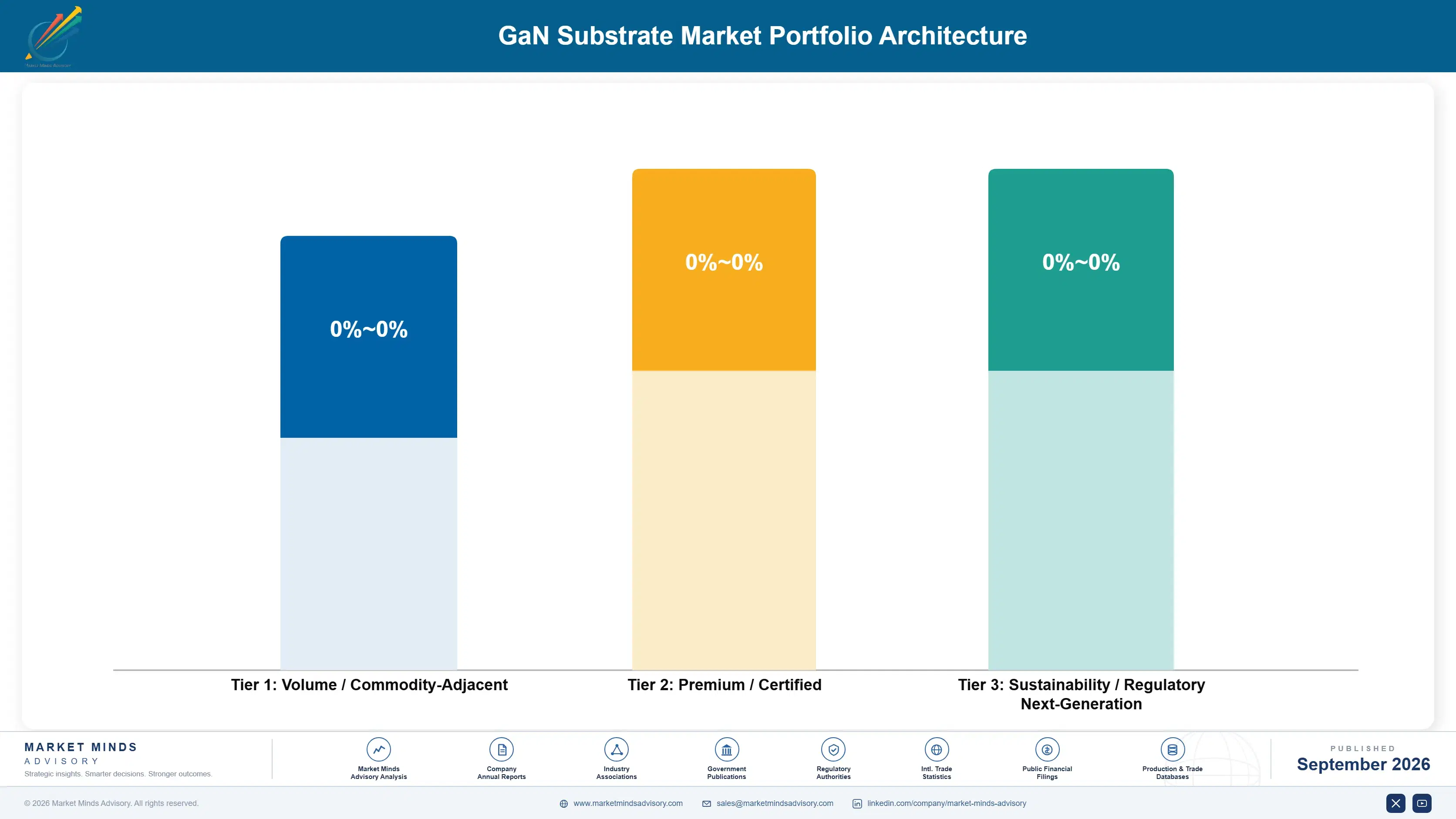
Portfolio Architecture for Margin Defence

Margin architecture in this market is unusually stark. Gallium nitride on sapphire earns least, on capacity built for LEDs and now competing on price. Gallium nitride on silicon sits above it on volume and thin margin. Bulk substrates of every growth route earn most, because area is trivial, value per wafer is enormous and there are perhaps six organisations anywhere capable of supplying them.
The volume versus premium tension here is not really a choice. Epitaxial capacity is capital equipment that can be ordered and installed, so anybody with money can enter and Chinese producers have. Bulk crystal growth is accumulated knowledge that cannot be ordered at all, which is why the same six names have held it for decades. A producer in the volume half cannot simply decide to move upward; that takes a decade or an acquisition.

High-value pools concentrate in ammonothermal bulk material and in gallium nitride on silicon carbide for defence radar, and neither is reached by adding capacity. Ammonothermal requires pressure vessel expertise and patience measured in months per boule. Radar material requires qualification measured in years. Both barriers are time rather than money, which is why capital alone has repeatedly failed in either.

Volume / Commodity-Adjacent

Gallium nitride on sapphire epitaxial wafers, on capacity originally built for LEDs and now competing hard on price. The eight point spread separates producers with converted LED lines already depreciated from those still carrying capital cost.
Gross Margin: 18% to 26%

Premium / Certified

Gallium nitride on silicon and on silicon carbide epitaxial wafers, sold into power conversion and qualified defence radar positions respectively. The twelve point spread reflects how much of a producer's book sits in qualified programmes rather than in competitive power conversion supply.
Gross Margin: 34% to 46%

Sustainability / Regulatory / Next-Generation

Freestanding bulk gallium nitride substrates by ammonothermal, hydride vapour phase and sodium flux routes, where perhaps six organisations anywhere can supply. The fourteen point spread reflects growth rate achieved, which differs enormously between producers and decides cost per wafer entirely.
Gross Margin: 58% to 72%
gan-substrate-market-portfolio-architecture-1789986983180

High-value Sub-segments and Strategic Watch-out

Ammonothermal Bulk GaN Substrates

Grows at 20.7% from a small base, on the only route producing defect density four orders of magnitude below epitaxial material. The fourteen point spread reflects achieved growth rate. Throughput at roughly 30 microns daily is the sole obstacle to volume here, and it always was.
Gross Margin: 58% to 72%

GaN-on-Silicon Epitaxial Wafers

Grows at 17.4% and carries almost all the volume, on power conversion demand from chargers, data centre supplies and solar inverters. The twelve point spread reflects yield. This is the half of the market where capacity can be bought rather than developed, and Chinese producers have bought heavily.
Gross Margin: 34% to 46%

HVPE Freestanding Bulk GaN Substrates

Grows at 15.6% supplying laser diode makers who have no alternative material at any price. The fourteen point spread reflects boule yield and reclaim discipline. Deposition based growth inherits defects from the seed, which caps how far this route can improve on quality at all.
Gross Margin: 58% to 72%

GaN-on-Sapphire Epitaxial Wafers

Grows at 8.4%, slowest of the six classes, on LED capacity now competing for whatever power and radio frequency work it can win. The eight point spread separates depreciated lines from those still carrying capital. Producers hold the capacity because scrapping it recovers nothing at all.
Gross Margin: 18% to 26%

How Wafer Demand Actually Locks

The annuity here is qualification rather than any supply agreement. A substrate qualified into a device process ships for that process's life, because requalifying means requalifying the device, and for a defence radar programme that means requalifying the radar. Qualification cycles run several years and programme lifetimes run decades, so a position won in 2020 is still shipping in 2040 and nobody is negotiating it annually.
Stickiness varies enormously by vertical. Defence radar is the deepest, where a supplier change requires programme level requalification nobody undertakes voluntarily. Automotive is close behind on similar logic across a shorter product life. Consumer power conversion is the shallowest: a charger manufacturer switches epitaxial wafer supplier on price with a few months of validation, which is why that half of the market earns so little.

The buyer has changed generationally and most suppliers have not noticed. Fifteen years ago the customer was an LED manufacturer buying sapphire epitaxy on price and volume. Today it is a power device designer who cares about defect density and thermal conductivity, or a defence prime who cares about qualification records above everything. Selling area to the first buyer while the second specifies is a common error.
gan-substrate-market-end-use-penetration-index-1789986983672

Where The Wafer Money Is

These are among the four positions where our research anticipates prominent divergence between winners and laggards over the coming forecast period. Each is grounded in the demand model, the regulatory perimeter, and the announced capacity pipeline.
01 / CRYSTAL GROWTH INVESTMENT

Buy Growth Rate, Not Growth Capacity

Ammonothermal growth adds roughly 30 microns a day, so a usable boule takes months in a pressure vessel that few organisations anywhere know how to operate safely. Every increment in growth rate converts directly into wafers per vessel per year against capital that is already sunk, which means doubling the rate roughly halves cost per wafer without buying a single additional vessel. The method already delivers defect density four orders of magnitude below epitaxial material, so throughput is the only thing standing between this route and genuine volume.
02 / QUALIFIED POSITION DEFENCE

Defend Radar Sockets Above Everything Else

Gallium nitride on silicon carbide for defence radar compounds at 12.9% on modest wafer area at very high value per square inch, and the qualification cycle runs several years. Once an amplifier module is qualified into a programme, nobody requalifies a substrate supplier to save material cost, because requalification exceeds any conceivable saving and programme lifetimes run decades. That is the exact opposite of the volume epitaxy business in every respect that matters, and defence procurement expands on political timescales rather than commercial ones.
03 / DIAMETER PROBLEM ENGINEERING

Engineer Around The Crystal, Not Through It

Commercial freestanding gallium nitride is still at 2 inches while silicon runs at 300 millimetres, and every doubling of diameter roughly quarters the substrate cost per die. Gallium nitride does not melt at accessible pressure, so the Czochralski pulling that made large silicon boules cheap is simply unavailable and every alternative route is slower and smaller. An engineered composite substrate bonding good material onto a cheap large carrier delivers much of the benefit and sidesteps a problem that has resisted thirty years of direct effort.
04 / GALLIUM SUPPLY SECURITY

Qualify Metal Outside The Chinese Channel

China introduced export controls on gallium in 2023 and the effect was immediate, because refining is concentrated there almost completely and precursors carry around 18% of epitaxial wafer cost. A Chinese producer buys the metal domestically with no export licence involved, while a Japanese, European or American producer buys the same material through a controlled channel at whatever it costs that quarter. Recovery from bauxite residues and zinc refining exists at small scale outside China and costs more, which is what security costs.

Engagement Snapshot From the Field

A live engagement with an industry participant carrying material or product regulatory and market exposure ahead of a defining policy shift, showing how our research translates into a defensible multi-year portfolio strategy.
MARKET MINDS ADVISORY · CLIENT ENGAGEMENT SUMMARY
GaN Substrate Producer Strategic Portfolio Review and Transition Roadmap 2026·Investment Scenario on GaN Substrate Exposure Evaluation 2025-26
CLIENT PROFILE
A European compound semiconductor device manufacturer producing gallium nitride power and radio frequency devices for automotive and defence customers, buying epitaxial wafers from three suppliers across two continents. Board pressure to secure supply had produced a proposal to build epitaxial capacity internally at considerable cost. Nobody had established whether the supply risk actually sat where the board assumed it did.
STRATEGIC CHALLENGE
Manufacturing wanted internal epitaxial capacity for security of supply. Finance objected that the capital would earn nothing against wafers available commercially at competitive prices. Neither side had traced the actual dependency, which turned out to sit upstream of epitaxy entirely, in gallium metal refining rather than in wafer deposition. The board decision was scheduled and the analysis did not exist.
MMA APPROACH
MMA traced the supply chain from finished device back to refined gallium metal, mapping which steps had alternative sources and which did not. We modelled the cost and lead time of internal epitaxial capacity against qualified multi-sourcing, and tested both against a gallium export restriction scenario. The work drew on 47 expert interviews conducted in Q4 2025 with substrate producers, refiners and comparable device manufacturers.
KEY FINDINGS
  1. Epitaxial wafer supply had 4 credible alternative sources at acceptable specification, so the dependency the board feared did not exist at that step.
  2. Refined gallium metal had 1 realistic source region, and every supplier under consideration bought from it, which made the multi-sourcing strategy considerably less protective than it appeared.
  3. Internal epitaxial capacity would have taken 3 years to qualify and would not have removed the gallium exposure at all (client-reported, unverified by MMA).
  4. Qualifying a non-Chinese gallium recovery source added roughly 6% to precursor cost and could be completed within a year (client-reported, unverified by MMA).
CLIENT PROFILE
A European compound semiconductor device manufacturer producing gallium nitride power and radio frequency devices for automotive and defence customers, buying epitaxial wafers from three suppliers across two continents. Board pressure to secure supply had produced a proposal to build epitaxial capacity internally at considerable cost. Nobody had established whether the supply risk actually sat where the board assumed it did.
STRATEGIC CHALLENGE
Manufacturing wanted internal epitaxial capacity for security of supply. Finance objected that the capital would earn nothing against wafers available commercially at competitive prices. Neither side had traced the actual dependency, which turned out to sit upstream of epitaxy entirely, in gallium metal refining rather than in wafer deposition. The board decision was scheduled and the analysis did not exist.
MMA APPROACH
MMA traced the supply chain from finished device back to refined gallium metal, mapping which steps had alternative sources and which did not. We modelled the cost and lead time of internal epitaxial capacity against qualified multi-sourcing, and tested both against a gallium export restriction scenario. The work drew on 47 expert interviews conducted in Q4 2025 with substrate producers, refiners and comparable device manufacturers.
KEY FINDINGS
  1. Epitaxial wafer supply had 4 credible alternative sources at acceptable specification, so the dependency the board feared did not exist at that step.
  2. Refined gallium metal had 1 realistic source region, and every supplier under consideration bought from it, which made the multi-sourcing strategy considerably less protective than it appeared.
  3. Internal epitaxial capacity would have taken 3 years to qualify and would not have removed the gallium exposure at all (client-reported, unverified by MMA).
  4. Qualifying a non-Chinese gallium recovery source added roughly 6% to precursor cost and could be completed within a year (client-reported, unverified by MMA).
RECOMMENDED STRATEGY
Phase 1: Phase one: abandon the internal epitaxial capacity proposal, since four credible wafer sources already exist and the capital would remove no real exposure. Phase 2: Phase two: qualify a non-Chinese gallium recovery source and accept the 6% precursor cost increase as the price of actual supply security. Phase 3: Phase three: trace every remaining input back to its refining step rather than its immediate supplier, since dependency hides one level upstream.
OUTCOME
The manufacturer shelved the epitaxial capacity proposal and redirected a fraction of the capital toward qualifying an alternative gallium source (client-reported, unverified by MMA). Supply security improved measurably while capital spending fell sharply. The board now requires every supply risk paper to trace dependency to the refining step, which is the finding that outlasted the engagement.

Frequently Asked Questions

Foundational context covering the market sizes, CAGR, scope, country, region and competition that inform every finding below. This section is provided to cover basics and most often pre-purchase conversations, answered from the MMA Primary Research Dataset.

What is the current size of the GaN Substrate Market?

Global value reaches USD 1.02 billion in 2026, measured as substrate and epitaxial wafer shipment area converted to revenue. The 2025 base is USD 0.9 billion.

How large will the GaN Substrate Market be by 2036?

Shipment value reaches USD 3.72 billion by 2036, an increase of USD 2.70 billion over the forecast period. That represents 3.65 times expansion from the 2026 base.

What is the CAGR for the GaN Substrate Market 2026 to 2036?

The base case runs at 13.8% annually, with a bull case at 15.2% if ammonothermal growth reaches commercial throughput and a bear case at 12.5% if Chinese epitaxial capacity outruns device demand.

Which segment is growing fastest?

Ammonothermal bulk gallium nitride substrates grow at 20.7%, half again the market rate of 13.8%. Growing a crystal in supercritical ammonia is the one route that could close the price gap against foreign substrates.

Who are the major companies in the GaN Substrate Market?

Sumitomo Chemical, Mitsubishi Chemical Group, Sumitomo Electric Industries, Coherent and Kyocera lead on shipment area, together holding 68%. Soitec, IQE and Innoscience hold smaller positions.

Which country is growing fastest?

China leads at 18.9%, converting epitaxial capacity built for LEDs toward power and radio frequency material with state funding behind it. India follows on new fabrication investment.

Report Segmentation Architecture

The full report scope spans multiple orthogonal segmentation dimensions, with cross-tabulated demand data provided for each dimension pair. Coverage extends further to regional breakdowns, trend trajectories, and the competitive detail needed to support segment-level decision-making.

By Substrate Construction

  • Ammonothermal Bulk GaN Substrates
  • GaN-on-Silicon Epitaxial Wafers
  • HVPE Freestanding Bulk GaN Substrates
  • GaN-on-Silicon Carbide Epitaxial Wafers
  • Sodium Flux And Other Bulk GaN Substrates
  • GaN-on-Sapphire Epitaxial Wafers

By End-Use Industry

  • Power Conversion And Charging
  • Defence Radar And Electronic Warfare
  • Telecommunications Infrastructure
  • Laser Diodes And Photonics
  • Automotive Electrification
  • Lighting And Display

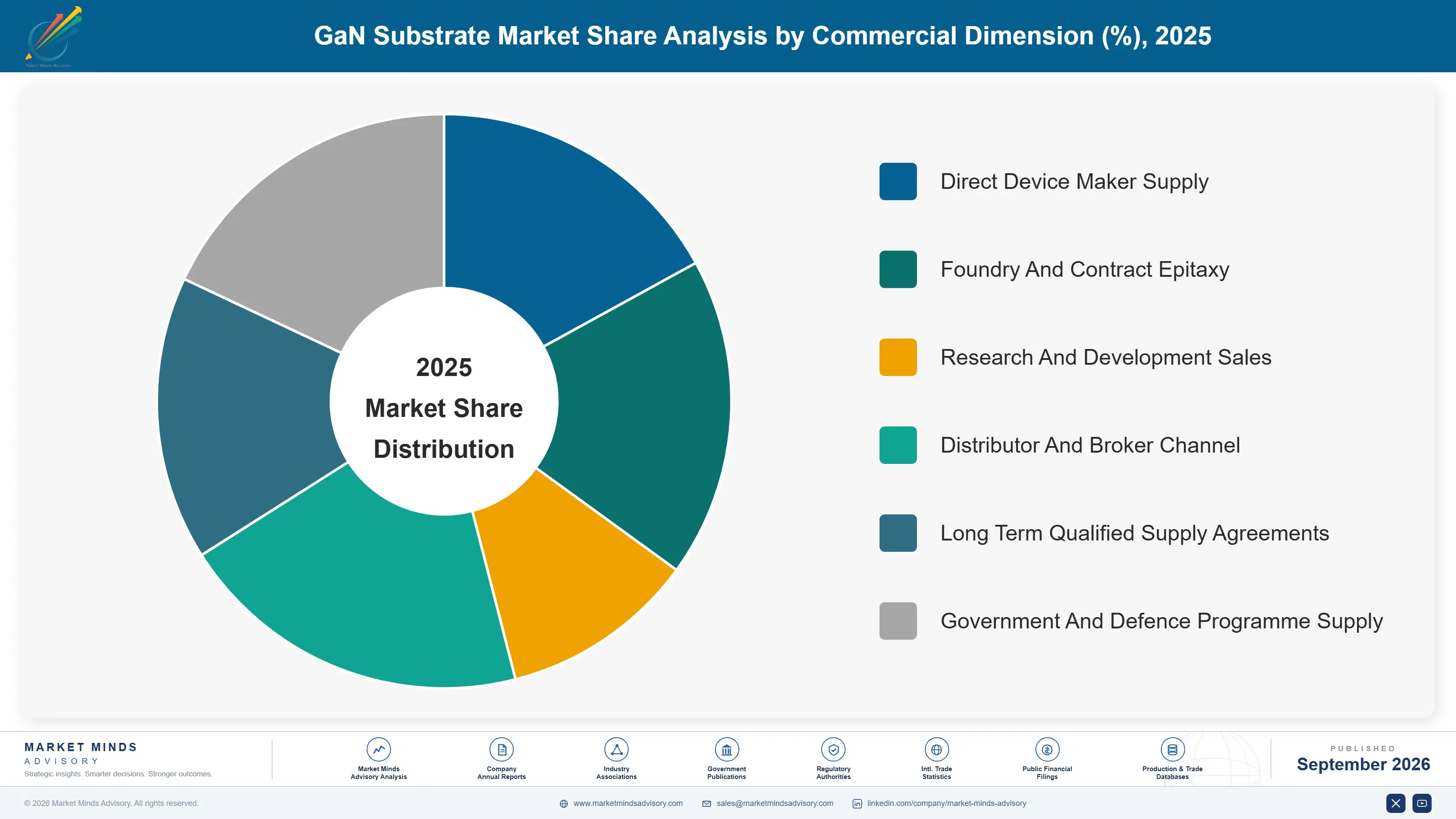
By Commercial Dimension

  • Direct Device Maker Supply
  • Foundry And Contract Epitaxy
  • Research And Development Sales
  • Distributor And Broker Channel
  • Long Term Qualified Supply Agreements
  • Government And Defence Programme Supply

By Region

  • North America
  • Western Europe
  • East Asia
  • South Asia and Pacific
  • Latin America
  • Middle East and Africa
  • Eastern Europe

Scope, Methodology, and Coverage

Every figure in this report is reproducible from documented input assumptions. The scope below maps the historical period, the forecast horizon, the segmentation dimensions, and the countries covered, alongside the underlying primary and qualitative methodology.
Historical Period
2020 to 2025
Forecast Period
2026 to 2036
Base Year
2025 (USD billions; MMA Primary Research Dataset, September 2026)
Market Definition
This report covers substrates on which gallium nitride devices are grown: gallium nitride on silicon, on silicon carbide and on sapphire epitaxial wafers, and freestanding bulk gallium nitride substrates grown by hydride vapour phase epitaxy, ammonothermal and sodium flux methods. It excludes finished gallium nitride devices, silicon carbide substrates for silicon carbide devices, bare sapphire and silicon wafers sold as commodity substrates, and epitaxial deposition equipment.
Quantitative Units
USD millions, substrate and epitaxial wafer shipment area basis; wafer area in square inches equivalent; defect density per square centimetre; substrate diameter in inches and millimetres; crystal growth rate in microns per day.
Segmentation Dimensions
Substrate construction; end-use industry; commercial supply channel; geography across seven regions.
Regions Covered
North America, Western Europe, East Asia, South Asia and Pacific, Latin America, Middle East and Africa, Eastern Europe
Countries Covered
Japan, China, Taiwan, South Korea, India, Australia, Singapore, United States, Canada, Mexico, Brazil, France, Germany, United Kingdom, Italy, Poland, Czechia, Romania, Israel, Egypt.
Key Companies Profiled
Sumitomo Chemical, Mitsubishi Chemical Group, Sumitomo Electric Industries, Coherent, Kyocera, Nichia, Soitec, IQE, Nanowin Technology, Sanan Optoelectronics, Enkris Semiconductor, Qromis, Furukawa Co., Ammono, Wolfspeed.
Quantitative Methodology
Primary survey, n=3,800 respondents, Q4 2025, six countries; demand-side model with trade association cross-validation
Qualitative Methodology
47 expert interviews, Q4 2025; applied to validate demand model assumptions, identify emerging dynamics, and assess competitive positioning
Report Format
PDF and XLSX data workbook (Word format preview document)
Publisher
Market Minds Advisory
Report Code
MMA-2026-CHM-211
Published
September 2026
Contact
sales@marketmindsadvisory.com | www.marketmindsadvisory.com

Purchase the full GaN Substrate Market Report (2026 to 2036).

This report sizes the global gallium nitride substrate market from 2026 to 2036 across six substrate constructions, six end-use industries and seven regions. It explains why almost every gallium nitride device is grown on foreign material, what the hundred times price gap against freestanding substrates costs in defect density, and why diameter has barely moved in thirty years. Cost composition is sourced to company annual reports, with gallium refining concentration analysed as the principal supply exposure. Regional analysis explains why East Asia holds 56% of shipment area with the technology and the volume in different countries. Competitive assessment covers 20 named suppliers with four revenue lever analyses.
Six substrate constructions sized through to 2036
Defect density and diameter economics modelled throughout
Gallium refining concentration analysed as supply exposure
Twenty named suppliers assessed on shipment area
Four revenue levers with quantified commercial impact
Anonymised European device maker sourcing engagement included

Built For The People Who Decide

From boardroom strategy to bench-side execution, this report is read cover-to-cover by leaders shaping the next decade of their industry, turning demand scenarios, market dynamics and valuation benchmarks into decisions.
CXOs/ Presidents/ VPs/ Managers
M&A and Corporate Development
Strategy Teams and R&D Heads
Procurement and Product Directors
Regulatory and Compliance Leaders
Investor Relations and Equity Analysts