Market Minds Advisory
EUV Lithography Market

EUV Lithography Market: High-NA Transition and Leading-Edge Capacity Concentration

AI accelerator and leading-edge logic demand is pulling foundries toward high numerical aperture EUV systems years earlier than planned, while single-supplier dependency and mask infrastructure readiness determine which fabs ship next-generation nodes on schedule.

Lead Analyst

David Horsley

Published

September 2026

Make Smarter Decisions with Customized Research Insights

Request a free sample report and evaluate market opportunities, growth trends, and competitive dynamics relevant to your business needs.

2025 MARKET VALUE$16.5BMarket Size 2025
2036 FORECAST VALUE$49.5BBase Case , 2026 to 2036
CAGR 2026 TO 203610.5 %Bull 11.8% / Bear 9.2%
INCREMENTAL OPPORTUNITY$31.2BNet 10- year value creation
EXPANSION MULTIPLE2.71x2036 value over 2026 base
Strategic Levers
M&A Pipeline
Regional Outlook
Country Rankings
Competitive Intelligence
Segmental Deep-dive
Call-Us : 91 93563 13602

Executive Snapshot and Market Trajectory

EUV lithography has moved from a leading-edge curiosity to the single scarcest resource in advanced chipmaking. Tool allocation, not chip design talent or wafer capacity, now determines which foundries can credibly promise next-generation process nodes, and fab roadmaps increasingly get built around confirmed system delivery slots.
High-NA EUV systems are growing at roughly 2.1x the broader market average as leading foundries pull forward adoption to meet AI accelerator and advanced packaging demand years ahead of prior roadmaps. East Asia has extended its dominance in both installed base and forecast growth, anchored by Taiwan's and South Korea's leading-edge capacity expansion, while North American fabs work to narrow the gap through new state-backed capacity investment programmes now scaling quickly.
Competitive intensity in the core exposure tool market remains almost entirely theoretical, since a single supplier controls system production, but real competitive activity plays out fiercely across pellicles, photoresist chemistry, and metrology, where several specialty materials suppliers compete for qualification slots. Mask infrastructure readiness and pellicle yield increasingly gate how fast fabs can actually convert tool capacity into shipped wafers each quarter. Regulators are increasingly monitoring these allocation dynamics given their rising strategic importance today.
Market Definition
The EUV lithography market covers extreme ultraviolet lithography systems, including low numerical aperture and high numerical aperture platforms, alongside directly bundled pellicles, service contracts, and metrology and inspection tools sold to semiconductor fabrication customers. It spans logic, foundry, and memory chipmakers adopting EUV patterning for leading-edge process nodes. Photoresist chemistry sold independently of system contracts and non-EUV deep ultraviolet lithography tools are excluded.
Base Year Value
$16.5B in 2025 (MMA Primary Research Dataset, August 2026)
Forecast Period
2026 to 2036, eleven discrete annual values
CAGR
10.5% base case. Bull 11.8%. Bear 9.2%.
Fastest Growth Segment
High-NA EUV Systems: 22.0% CAGR
Fastest Growth Country
Taiwan: 14.8% CAGR
Fastest Growth Region
South Asia and Pacific: 12.7% CAGR
Largest Region
East Asia: 30% of 2025 global value
Market Leaders
ASML Holding, Carl Zeiss SMT, JSR Corporation, Shin-Etsu Chemical, KLA Corporation. Source: MMA Analysis based on company annual reports.
Primary Survey
n=3,800 procurement and R&D decision-makers, Q4 2025, six countries
Methodology
Demand-side build-up, cross-validated against public data, 47 expert interviews

EUV Lithography Market Forecast Scenarios

euv-lithography-market-size-forecast-scenario-1787302246677
Between 2020 and 2025 the market expanded at an estimated 9.5% historical CAGR, driven by the initial ramp of 0.33 NA systems across leading foundry and memory customers. Growth accelerated meaningfully from 2023 onward as generative AI accelerator demand pulled forward capacity expansion plans that had previously been paced more conservatively across the industry, each new fab announcement adding to an already crowded order backlog.
The base case assumes 10.5% CAGR through 2036, resting on three mechanisms: high-NA system adoption ramping across leading foundries chasing sub-2 nanometer nodes, memory manufacturers extending EUV layer counts deeper into DRAM production to sustain density scaling, and service and upgrade contract revenue compounding as the installed base of low-NA systems ages into its retrofit window. Expanding advanced packaging applications for EUV patterning add a reinforcing tailwind, broadening the addressable customer base beyond pure logic manufacturing over the decade ahead.
A bull scenario, near 11.8% CAGR, assumes faster than expected high-NA qualification and accelerated fab construction in the United States pull system deliveries forward. The bear case, near 9.2%, assumes memory and logic capital spending slows amid a cyclical semiconductor downturn, pushing some fabs to delay high-NA orders and extend existing low-NA tool utilization instead.

Tool Allocation Now Gates the Entire Leading-Edge Roadmap

Three forces are converging on EUV demand simultaneously: an AI-driven leading-edge capacity race that rewards whichever fab secures tool allocation first, a parallel high-NA transition that is reshaping capital budgets years ahead of prior roadmap assumptions, and a mask and pellicle infrastructure buildout racing to keep pace with exposure tool throughput. Fabs increasingly negotiate allocation years before a tool ships, treating delivery slot certainty as more valuable than marginal price con
MARKET CONCENTRATION78%Combined revenue share held by top five suppliers
SYSTEM ASP$380MBlended selling price for a high-NA exposure system
ORDER-TO-DELIVERY LEAD TIME18-24 moTypical wait time between system order and installation
FAB UTILIZATION91%Share of installed EUV tool hours running production
TOP DEPLOYMENT COUNTRYTaiwanLeading country for installed EUV exposure tool count
PELLICLE YIELD RATE88%Share of high-NA pellicles passing qualification on first pass
Commercially, the category functions less like an equipment sale and more like a multi-year capacity allocation relationship. Customers commit capital and engineering resources years in advance of delivery, and the supplier increasingly determines which fabs receive priority based on strategic partnership depth rather than order size alone. Materials suppliers serving pellicles and photoresist compete for qualification slots that, once won, tend to persist for the full life of a process node.
Over the next decade, expect high-NA systems to displace low-NA orders at the leading edge, continued tight coupling between system delivery schedules and fab construction timelines, and growing government intervention as EUV access becomes explicitly tied to national semiconductor strategy and export control policy across multiple jurisdictions simultaneously.
"Everyone frames this as a chip shortage story. It's really a lithography allocation story wearing a chip shortage costume, and the fabs that understood that two years ago are the ones shipping on schedule now."
Director, Semiconductor Capital Equipment Practice · MMA Semiconductor Capital E

Market Trends

High-NA Systems Enter Volume Production Ramp

Leading foundries and memory manufacturers are moving high-NA EUV systems from pilot line evaluation into early volume production faster than most roadmaps anticipated even two years ago, driven by the density and overlay accuracy advantages high-NA optics provide for sub-2 nanometer logic nodes. Each high-NA system requires a substantially larger cleanroom footprint and power infrastructure than its low-NA predecessor, forcing fabs to plan facility construction years ahead of tool delivery rather than retrofitting existing bays. Suppliers report order backlogs extending several years, and customers increasingly negotiate allocation priority through long-term strategic partnership agreements rather than standard purchase orders alone.
Market Impact: Adds 45 new tool orders yearly
Mask and Pellicle Infrastructure Becomes the New Bottleneck

As exposure tool throughput increases, mask blank supply and high-NA pellicle yield have emerged as the binding constraint on how quickly fabs can convert installed tool capacity into shipped wafers, since a single unqualified pellicle can force costly production delays. Pellicle suppliers are racing to scale production of ultra-thin, high-transmission membranes capable of surviving increased power densities without degrading pattern fidelity across a full production lot. Fabs report qualifying a new pellicle supplier can take upward of a year, making incumbent pellicle relationships nearly as commercially valuable as the exposure tool contracts they support directly today.
Market Impact: Adds 6 new qualified fab sites

Market Opportunities and Growth Drivers

AI Accelerator Demand Pulls Forward Leading-Edge Capacity

Generative AI training and inference chip demand is pushing leading foundries to expand sub-3 nanometer capacity far faster than prior semiconductor cycles, and each new leading-edge fab module requires multiple EUV exposure tools to reach designed wafer output. Foundry customers report capacity commitments booked several years in advance, reflecting confidence that AI accelerator demand will absorb capacity that in earlier cycles might have taken considerably longer to fill. This compressed timeline is straining supplier production capacity, since building a single exposure tool requires assembling hundreds of thousands of precision components sourced from a tightly qualified supply base.
Market Impact: Concentrates 100% share in 1 firm

National Semiconductor Strategy Programmes Fund New Fab Construction

Government incentive programmes across the United States, Japan, and the European Union are funding new leading-edge fab construction explicitly designed to reduce geographic concentration of advanced chipmaking capacity, and each qualifying fab requires EUV tool orders as a prerequisite for reaching advertised process node targets. Export control policy is simultaneously restricting which countries can purchase EUV systems at all, concentrating available tool allocation among an approved customer list that is expanding more slowly than underlying chip demand. Suppliers report these policy dynamics increasingly shape order sequencing as much as customer readiness or payment terms do.
Market Impact: Raises entry capex by roughly 60%

Market Restraints and Challenges

Single-Supplier Dependency Creates Systemic Delivery Risk

The exposure tool market depends on a single qualified supplier for the most advanced systems, and the root cause is the extraordinary precision engineering barrier involved in EUV optics and light source technology that took decades and tens of billions of dollars to develop. The commercial impact falls hardest on fabs whose expansion timelines depend on a single delivery slot, since any supplier-side production delay cascades directly into delayed process node launches with no alternative qualified source available. Customers are mitigating this exposure by booking capacity years earlier than necessary.
Market Impact: Adds 22% CAGR to high-NA segment

High-NA Capital Cost Strains Mid-Tier Fab Budgets

High-NA system pricing sits meaningfully above low-NA predecessors, and the root cause is the substantially larger and more precise optical assembly required to achieve the tighter overlay accuracy high-NA lithography delivers at advanced nodes. The commercial impact concentrates hardest on mid-tier foundries and memory manufacturers without hyperscaler-backed capital budgets, some of which are delaying high-NA adoption and extending low-NA tool life through multi-patterning workarounds instead. Suppliers are mitigating this exposure by offering extended financing terms and phased delivery schedules that spread capital outlay across a longer commissioning timeline. Some analysts expect this gap to narrow only gradually.
Market Impact: Limits throughput gains to 12% year
3 additional market trends, 3 additional growth drivers, and 2 additional restraints and challenges are covered in the full report. Contact sales@marketmindsadvisory.com to access the complete intelligence.

Segment CAGR and Growth Architecture

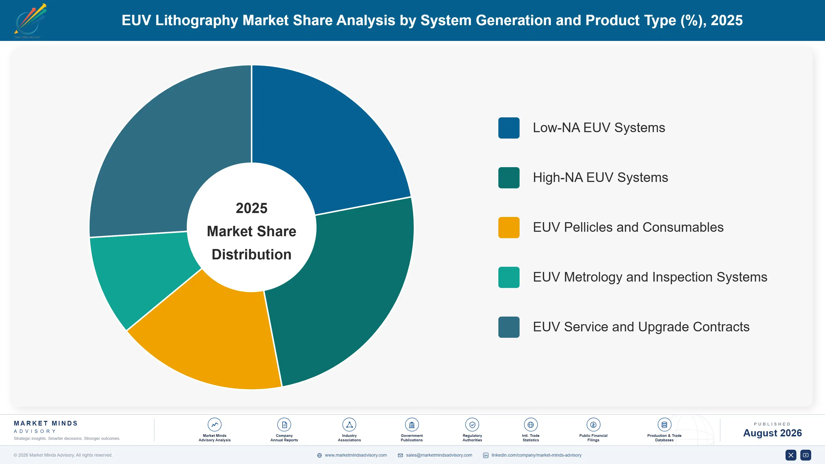
Segmentation follows system generation and product type, the dimension fabs specify against when planning capacity and capital budgets. Low-NA and high-NA exposure systems, pellicles and consumables, metrology and inspection tools, and service contracts each serve a distinct stage of the lithography workflow, keeping tool hardware and materials dimensions separate across both hardware and consumables product categories.
euv-lithography-market-market-share-analysis-1787302247557

High-NA EUV Systems

High-NA systems use a larger, more precise optical assembly to deliver tighter overlay accuracy than low-NA predecessors, enabling single-exposure patterning at process nodes that would otherwise require costly multi-patterning workarounds using older tools. Adoption is concentrated among leading foundries and memory manufacturers racing to reach sub-2 nanometer logic and next-generation DRAM density targets ahead of competitors. Growth outpaces the broader EUV market by roughly 2.1x as customers pull forward capital budgets to secure early delivery slots, treating allocation priority as a durable competitive advantage independent of unit pricing. Facility construction requirements, including larger cleanrooms and expanded power infrastructure, are forcing customers to commit to fab buildouts years before a single tool actually arrives on site and begins production qualification.
CAGR 22.0%

EUV Pellicles and Consumables

Pellicles protect EUV photomasks from particle contamination during exposure, and demand is rising sharply as high-NA systems require thinner, higher-transmission membranes capable of surviving greater power densities without degrading pattern fidelity across a production lot. Growth is fastest among suppliers who have successfully qualified pellicles for high-NA tool generations, since qualification cycles can take upward of a year and create durable incumbency once achieved. Fabs increasingly treat pellicle supply relationships as strategically important as the exposure tool contracts they support, given that a single yield problem can halt an entire production lot. Suppliers with proven high-NA qualification are capturing outsized commercial value relative to their historical share of the broader consumables category.
CAGR 11.5%
Full segment breakdown across 5 segments available in the complete report.

Regional Architecture and Country Demand Map

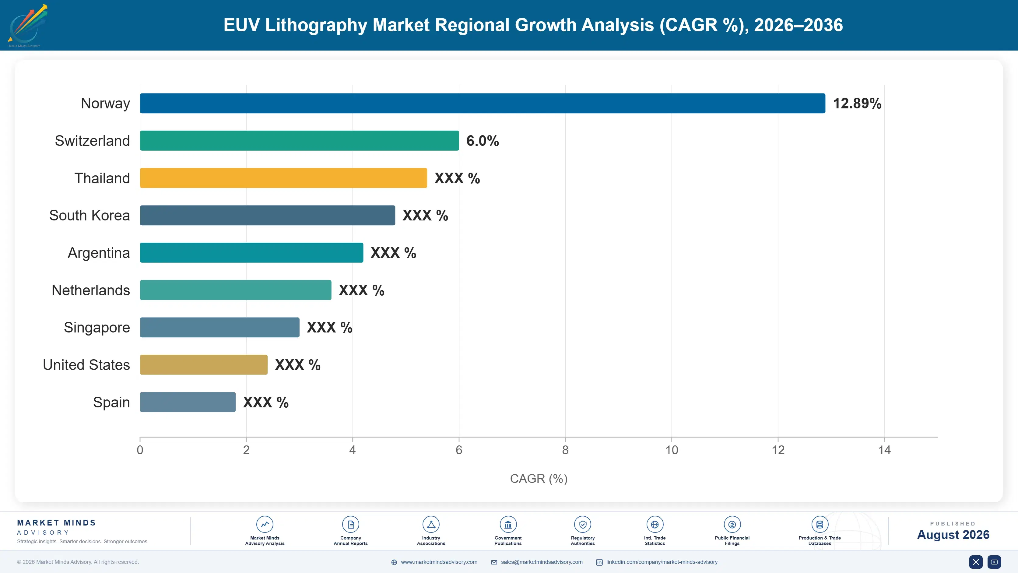
East Asia holds the largest and fastest-growing share as Taiwan's and South Korea's leading foundries and memory makers expand leading-edge capacity, while North America narrows the gap through state-backed fab construction and export-control-driven onshoring initiatives now underway. Western Europe retains deep technical influence through its optics and component manufacturing base.

North America

United States leading-edge fab construction, funded partly through federal semiconductor incentive programmes, is driving the region's fastest EUV tool order growth as foundries and memory makers race to reach announced capacity targets across Arizona, Ohio, and Texas. Domestic fabs increasingly compete directly with Asian counterparts for the same limited pool of annual exposure tool deliveries, a dynamic that did not exist a decade ago when leading-edge capacity was overwhelmingly concentrated offshore. Export control policy further shapes regional demand, since restrictions on tool sales to certain markets indirectly redirect available allocation toward approved American and allied customers. Growth trails East Asia because the region's leading-edge fab base remains smaller in absolute installed tool count despite its faster expansion rate.
Share: 26% | CAGR: 11.3% (2026 to 2036)

Western Europe

Western Europe hosts the design, optics, and light source engineering base behind the exposure tool supply chain, giving the region deep technical influence even though leading-edge fab deployment within Europe itself remains comparatively limited. German and Dutch specialty materials and component suppliers continue expanding capacity to keep pace with exposure tool production schedules, capturing meaningful value even without hosting large-scale chip fabrication themselves. European Union semiconductor sovereignty initiatives are funding early-stage leading-edge fab construction aimed at reducing the region's reliance on imported advanced chips, though these projects remain earlier in their build timeline than comparable American and Asian efforts. Growth trails the global rate as the region's own fab deployment ramp lags its component and optics manufacturing strength considerably.
Share: 20% | CAGR: 9.0% (2026 to 2036)
Regional intelligence for 5 additional markets available in the complete report: East Asia, South Asia and Pacific, Latin America, Middle East and Africa, Eastern Europe. Contact sales@marketmindsadvisory.com.
euv-lithography-market-country-cagr-analysis-1787302248395

Monetizing Allocation Priority and Lifecycle Services

Suppliers across the value chain are shifting commercial emphasis from one-time tool or material sales toward long-term allocation agreements, qualification partnerships, and lifecycle service contracts, since fabs now value delivery certainty and technical partnership depth as much as unit pricing itself. This mirrors a broader shift across capital equipment toward relationship-based commercial structures consistently.

Structuring Long-Term Priority Capacity Allocation Agreements

The leading exposure tool supplier increasingly structures multi-year strategic partnership agreements that guarantee delivery slot priority in exchange for customer capital commitments made years before a tool actually ships, formalizing a practice that was informal in earlier industry cycles. This shifts commercial risk toward customers, who must commit capital ahead of confirmed demand visibility, while giving the supplier multi-year production planning certainty across its component supply base. Strategic partners report receiving priority allocation worth an estimated 12 to 18 months earlier delivery than standard order customers, a meaningful competitive advantage in a market where process node timing determines customer wins.
Market Impact: Secures delivery slots 12 to 18 mon

High-NA Field Upgrade and Retrofit Programs

Suppliers are increasingly offering field upgrade packages that extend low-NA system capability through improved light sources and overlay correction software, giving fabs a lower-cost bridge option before committing to a full high-NA system purchase. This service layer extends the productive life of an installed low-NA tool by an estimated 3 to 4 years beyond its original planned retirement, deferring a major capital outlay for budget-constrained customers. Suppliers report upgrade program attach rates rising steadily among mid-tier foundries unable to justify immediate high-NA capital commitments, converting what was previously idle installed base into incremental service revenue.
Market Impact: Extends tool life by roughly 3 to 4

Early Pellicle and Consumables Qualification Co-Development

Materials suppliers are increasingly co-developing pellicle and photoresist formulations directly with fab process engineering teams well before a process node reaches production, securing qualification slots that then persist for the full commercial life of that node. This early co-development model shortens formal qualification cycles by an estimated 4 to 6 months versus a supplier submitting a finished product cold, a meaningful advantage when node timelines are compressed by competitive pressure. Suppliers with established co-development relationships report qualification win rates well above those competing purely on submitted sample performance after the fact.
Market Impact: Cuts qualification cycles by 4 to 6

Predictive Maintenance and Uptime Guarantee Contracts

Given how costly unplanned exposure tool downtime is to a fab's entire production schedule, suppliers are increasingly selling predictive maintenance contracts bundled with contractual uptime guarantees backed by real-time tool telemetry monitoring. Fabs report these contracts reduce unplanned downtime incidents by an estimated 25 to 35% versus reactive maintenance models, a meaningful improvement given that a single tool failure can idle an entire production lot worth tens of millions of dollars. Suppliers price uptime guarantee tiers at a meaningful premium over standard service contracts, and attach rates are highest among customers running the newest, least field-proven tool generations.
Market Impact: Cuts unplanned downtime by 25 to 35

Who Controls the Margin Pool

The top five suppliers hold roughly 78% combined share, an unusually high concentration even by semiconductor capital equipment standards, reflecting the fact that a single company controls exposure tool production entirely while the remaining share concentrates among specialty materials and metrology suppliers. The gap between the exposure tool monopoly and every other participant in the value chain is not merely wide, it is categorical, since no qualified alternative tool source currently exis
Current competitive activity concentrates on three fronts outside the tool monopoly itself: pellicle and photoresist qualification races for the high-NA transition, metrology and inspection precision improvements needed to support tighter overlay tolerances, and mask blank supply capacity expansion to keep pace with rising exposure tool throughput. Materials suppliers increasingly compete on co-development partnership depth rather than on submitted sample performance alone.

Emerging pressure comes less from new entrants challenging the exposure tool monopoly, which remains commercially and technically unassailable within the forecast horizon, and more from materials suppliers racing to qualify for the high-NA transition before incumbents lock in multi-year node relationships. Rankings among materials and metrology suppliers could shift meaningfully as high-NA qualification cycles complete, rewarding whichever suppliers invested earliest in high-NA-compatible product development.
euv-lithography-market-company-positioning-matrix-1787302249289

Competitive Moat and Risk Dimensions

ASML HOLDING

Moat: Exposure tool monopoly

ASML's multi-decade lead in EUV optics, light source, and precision motion control technology, built through tens of billions of dollars in cumulative research investment, gives it an effectively unassailable monopoly that no competitor has credibly challenged in over a decade of industry effort. That lead compounds with every new node.
ASML HOLDING

Risk: Geopolitical export exposure

ASML's sales depend heavily on export licensing decisions made by the Dutch and United States governments, and any tightening of restrictions on which customers can purchase EUV systems directly constrains addressable revenue regardless of underlying customer demand or available production capacity. That exposure is unlikely to ease soon.
KLA CORPORATION

Moat: Metrology precision leadership

KLA's decades of accumulated process control and defect inspection expertise give it durable incumbency as overlay tolerances tighten with each new node, since fabs rarely qualify a new metrology supplier without years of comparative field validation against KLA's established tool performance. That validation barrier compounds with every generation.
KLA CORPORATION

Risk: Indirect exposure tool dependency

KLA's growth remains tied to the pace of exposure tool deployment it does not control, meaning any slowdown in high-NA system shipments directly constrains the metrology and inspection capacity expansion that would otherwise drive KLA's own revenue growth. That dependency is unlikely to loosen further.

Players Tracked

Prominent Players

ASML Holding
Carl Zeiss SMT
JSR Corporation
Shin-Etsu Chemical
KLA Corporation

Other Key Players

Merck KGaA
Tokyo Electron
Lasertec Corporation
Fujifilm Electronic Materials
Tokyo Ohka Kogyo
Sumitomo Chemical
DuPont Electronics
Entegris
Applied Materials
Zeon Corporation
HOYA Corporation
Toppan Photomasks
Screen Holdings
Advantest
Hitachi High-Tech

Recent Developments

OCTOBER 2025

ASML Ships First High-NA System to Leading Foundry Customer

ASML completed shipment and installation of an early high-NA EUV system to a leading foundry customer's pilot production line, marking a milestone step toward volume high-NA adoption. The shipment reflects organic production output rather than any acquisition or joint venture, funded through ASML's ongoing capital expenditure programme.
Signal: Confirms high-NA transition timeline is ac
FEBRUARY 2026

Shin-Etsu Chemical Expands High-NA Pellicle Production Capacity

Shin-Etsu Chemical announced expanded production capacity for high-NA compatible EUV pellicles at its domestic Japanese facilities, aiming to address a qualification bottleneck several leading foundries have flagged publicly. The expansion is organic capacity growth, not an acquisition or joint venture, funded through existing capital investment programmes.
Signal: Highlights pellicle supply as an increasin
MAY 2026

KLA Corporation Acquires Advanced Overlay Metrology Startup

KLA Corporation completed the acquisition of a privately held overlay metrology startup, adding measurement technology specifically developed for high-NA overlay tolerance requirements to its existing inspection portfolio. The deal strengthens KLA's positioning ahead of accelerating high-NA volume production across leading customers worldwide. Terms of the transaction were not disclosed publicly.
Signal: Signals continued consolidation of special

Precision Optics and Light Source Component Exposure

Precision optics, light source components, and ultra-high-purity materials together represent an estimated 55 to 65% of exposure tool cost of goods sold, reflecting the extraordinary manufacturing tolerances required across thousands of individually qualified components. Optics supply remains effectively single-sourced through a long-standing strategic partnership, creating a supply base narrower than almost any other capital equipment category in semiconductors.
Tin droplet light source components experienced meaningful supply tightness during 2022 and 2023 as exposure tool production accelerated faster than the specialty component supply chain could scale, a constraint several suppliers disclosed in annual reports and investor presentations as a near-term production bottleneck. Component lead times reportedly stretched beyond forty weeks during the tightest period, forcing the exposure tool supplier to prioritize allocation among customers with the most advanced strategic partnership agreements already in place.

Smaller specialty materials suppliers carry disproportionate exposure to these input constraints since they lack the purchasing scale and strategic relationships that the largest suppliers maintain directly with precision component manufacturers. This gap is widest for newer entrants attempting to qualify high-NA compatible materials, leaving them more vulnerable to component allocation shortfalls than incumbents with decades of accumulated supplier relationship depth across the value chain.
euv-lithography-market-cost-volatility-analysis-1787302249670

Vertical Integration Into Critical Optics Components

The leading exposure tool supplier continues investing directly in owned and joint-venture precision optics production rather than relying solely on external component sourcing, insulating its production schedule from the component shortages that stretched lead times beyond forty weeks during 2022 and 2023 industry-wide. This also shields margin during future disruptions across multiple product lines.

Multi-Year Strategic Component Supply Agreements

Leading suppliers increasingly lock multi-year pricing and volume commitments directly with precision component manufacturers, smoothing input costs and insulating production schedules from the spot market volatility smaller specialty suppliers remain exposed to during periods of accelerating industry-wide demand. This practice has become standard procurement policy since 2023, reducing spot market exposure considerably for adopting suppliers.

Diversified Qualification Across Materials Suppliers

Fabs are increasingly qualifying a second pellicle or photoresist supplier alongside their primary relationship, avoiding total dependence on a single materials source that could otherwise halt production entirely during a supply disruption or unexpected yield problem at one supplier's facility. This flexibility also shortens future requalification timelines, giving fabs more resilience against a single supplier's unexpected quality failure.

Portfolio Architecture for Margin Defence

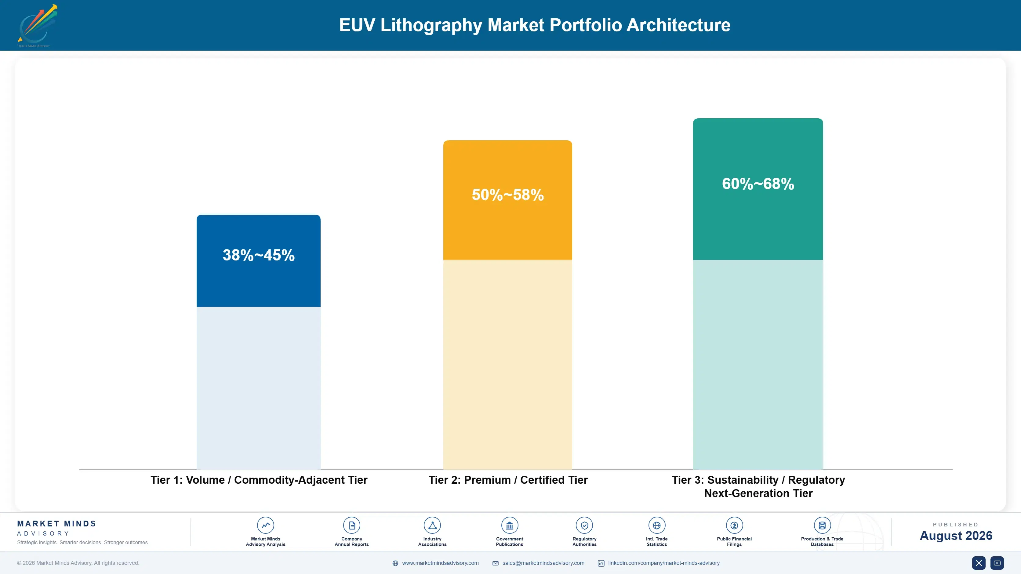
Portfolio architecture splits across three tiers: low-NA systems and standard consumables competing on established, largely stable pricing, certified high-NA-qualified materials and metrology tools carrying steep qualification barriers that support durable pricing, and next-generation high-NA systems bundled with strategic partnership and lifecycle service agreements. Gross margins widen meaningfully moving up this ladder as qualification and technical barriers concentrate hardest at the newest
The volume versus premium tension is comparatively muted at the exposure tool level given the single-supplier structure, but plays out sharply among materials suppliers, where established pellicle and photoresist qualification holders defend premium pricing while newer entrants compete aggressively on price to win their first qualification slot. High-NA-qualified materials retain the strongest pricing power because qualification cost and multi-year node relationships discourage fabs from switching suppliers mid-programme.

High value margin pools concentrate in high-NA systems and their associated qualified consumables base, where strategic partnership depth and lifecycle service contracts together support gross margins well above the portfolio average. Suppliers across the value chain are consequently prioritizing capital and engineering investment toward high-NA qualification even though it remains a minority of total installed base today, betting the mix shifts decisively within the decade ahead.

Volume / Commodity-Adjacent Tier

Low-NA systems and standard consumables serving established process nodes, competing on largely stable long-term pricing with limited near-term margin expansion potential across the mature installed base. Suppliers here compete mainly on price and delivery reliability.
Gross Margin: 38-45%

Premium / Certified Tier

Qualified metrology, inspection, and materials products serving advanced process nodes, where qualification cost and multi-year node relationships support durable, defensible pricing power across the value chain. Buyers rarely switch suppliers once a product is qualified.
Gross Margin: 50-58%

Sustainability / Regulatory / Next-Generation Tier

High-NA systems and their qualified consumables base, bundled with strategic partnership and lifecycle service agreements, sold on allocation certainty and technical partnership value rather than unit price. Suppliers here compete primarily on partnership depth and allocation certainty.
Gross Margin: 60-68%
euv-lithography-market-portfolio-architecture-1787302250557

Node Qualification Locks In Recurring Demand

EUV economics function like a multi-year annuity once a materials or metrology supplier wins qualification on a given process node, since that qualification typically persists for the full commercial life of the node, often five to seven years across multiple product generations built on the same process. This is why suppliers invest so heavily in early co-development relationships, treating qualification wins as a foothold rather than the primary profit event itself, since real revenue compound
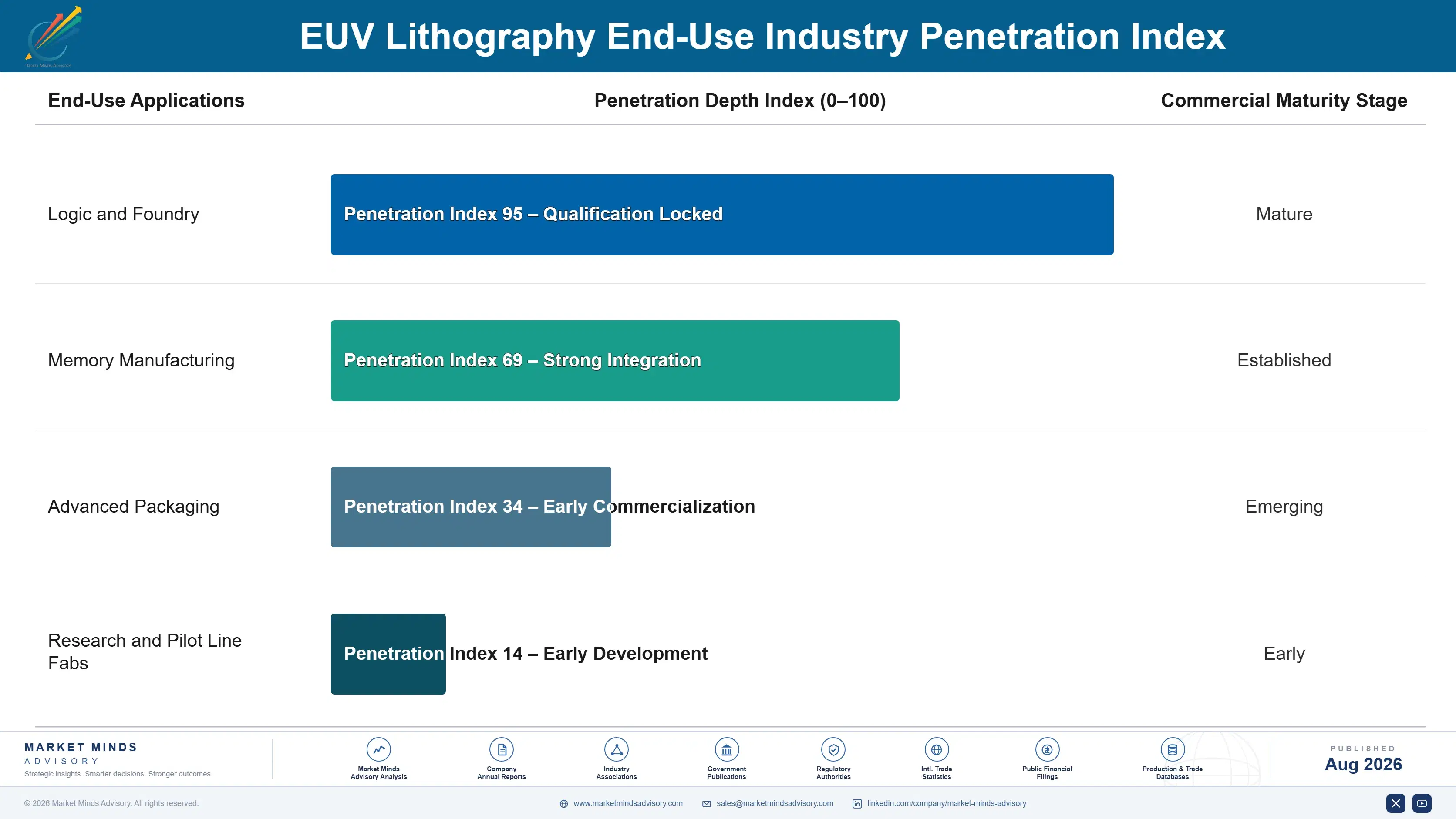
Adoption depth varies sharply by end-use vertical. Leading logic and foundry customers are pushing hardest into high-NA adoption to defend process node leadership, while memory manufacturers adopt more selectively, extending EUV layer counts gradually rather than converting entire process flows at once given more cost-sensitive economics across commodity memory products competing on thin per-bit margins.

Buyer profiles are shifting generationally as process integration engineers who trained primarily on EUV-native workflows increasingly influence fab capital planning decisions alongside veteran engineers who remember the multi-patterning era before EUV adoption. This is accelerating willingness to commit early to high-NA capital budgets even among historically conservative memory manufacturers who once waited for mature, de-risked technology before committing meaningful capital to a new tool generation.
euv-lithography-market-end-use-penetration-index-1787302251372

Where Leading-Edge Capital Strategy Should Focus

These are among the four positions where our research anticipates prominent divergence between winners and laggards over the coming forecast period. Each is grounded in the demand model, the regulatory perimeter, and the announced capacity pipeline.
01 / ALLOCATION PRIORITY STRATEGY

Secure high-NA delivery slots years before capacity is needed

Tool allocation, not capital availability, has become the binding constraint on leading-edge fab expansion, and customers who delay booking high-NA capacity risk losing multiple years of competitive positioning to rivals who committed earlier. Strategic partnership depth increasingly determines delivery sequencing more than order size or payment terms alone. Fabs that treat allocation booking as a routine procurement decision rather than a strategic priority risk finding themselves several years behind competitors who understood the stakes sooner and acted decisively, well before allocation windows closed.
02 / MATERIALS QUALIFICATION TIMING

Co-develop pellicles and photoresist ahead of node finalization

High-NA qualification slots for pellicles and photoresist are being locked in years before volume production begins, rewarding materials suppliers who invest in co-development partnerships with fab process teams well ahead of broader market demand signals. Suppliers waiting for a finished process node specification before beginning qualification work will find incumbents already entrenched. The commercial value of early qualification persists for the full life of a node, often five to seven years, making early investment durably valuable across multiple product generations.
03 / SUPPLY CHAIN RESILIENCE

Diversify materials qualification beyond a single supplier

The 2022 and 2023 component shortage demonstrated how a single tight link in the precision component supply chain can stretch lead times well beyond forty weeks during a disruption event affecting the entire industry. Fabs are increasingly qualifying a second materials supplier to avoid total production exposure to any single source failure or yield problem. Suppliers still dependent on a single customer relationship for the majority of their qualified revenue remain exposed to concentration risk that diversified competitors have already addressed.
04 / POLICY AND EXPORT EXPOSURE

Treat export control policy as a permanent planning input

Export control decisions increasingly determine addressable customer bases independent of underlying technical demand, and suppliers and fabs alike must treat policy shifts as a permanent planning input rather than a peripheral risk factor to monitor occasionally. Customers excluded from EUV access face a multi-year competitive disadvantage with no near-term technical substitute available at comparable performance. Suppliers serving approved customer lists should expect continued government scrutiny of allocation decisions as EUV access becomes further tied to national industrial strategy over time.

Engagement Snapshot From the Field

A live engagement with an industry participant carrying material or product regulatory and market exposure ahead of a defining policy shift, showing how our research translates into a defensible multi-year portfolio strategy.
MARKET MINDS ADVISORY · CLIENT ENGAGEMENT SUMMARY
EUV Lithography Producer Strategic Portfolio Review and Transition Roadmap 2026·Investment Scenario on EUV Lithography Exposure Evaluation 2025-26
CLIENT PROFILE
The client is a mid-tier foundry operating advanced process node capacity across two countries, generating revenue in the low single digit billions (client-reported, unverified by MMA). Facing intensifying competition from hyperscaler-backed leading foundries with deeper capital budgets, the client's existing exposure tool allocation lagged competitors by an estimated eighteen months, threatening its ability to credibly compete for next-generation customer design wins.
STRATEGIC CHALLENGE
Corporate leadership sought a revised capital allocation and supplier relationship strategy capable of closing the eighteen-month tool delivery gap against better-capitalized competitors, while avoiding capital commitments the client's balance sheet could not credibly sustain, ensuring near-term customer commitments remained fully protected throughout the entire multi-phase transition period under active review.
MMA APPROACH
MMA benchmarked the client's existing supplier relationship depth against five comparable foundries with faster allocation access, then modeled alternative capital commitment structures, including phased high-NA field upgrade adoption, designed to narrow the competitive gap without straining the client's balance sheet, reflecting the client's specific balance sheet constraints identified carefully during initial discovery sessions.
KEY FINDINGS
  1. The client's capital commitment timeline lagged the fastest-moving competitors by roughly fourteen months on average across comparable allocation negotiations reviewed in detail.
  2. Phased field upgrade adoption was projected to close roughly 60% of the competitive capacity gap without a full high-NA system order (client-reported, unverified by MMA).
  3. Strategic partnership depth, not order size alone, most strongly predicted allocation priority among the five foundries benchmarked in this carefully conducted analysis.
  4. Early materials co-development engagement was found to meaningfully improve qualification timeline outcomes independent of exposure tool allocation timing itself, for this specific engagement.
CLIENT PROFILE
The client is a mid-tier foundry operating advanced process node capacity across two countries, generating revenue in the low single digit billions (client-reported, unverified by MMA). Facing intensifying competition from hyperscaler-backed leading foundries with deeper capital budgets, the client's existing exposure tool allocation lagged competitors by an estimated eighteen months, threatening its ability to credibly compete for next-generation customer design wins.
STRATEGIC CHALLENGE
Corporate leadership sought a revised capital allocation and supplier relationship strategy capable of closing the eighteen-month tool delivery gap against better-capitalized competitors, while avoiding capital commitments the client's balance sheet could not credibly sustain, ensuring near-term customer commitments remained fully protected throughout the entire multi-phase transition period under active review.
MMA APPROACH
MMA benchmarked the client's existing supplier relationship depth against five comparable foundries with faster allocation access, then modeled alternative capital commitment structures, including phased high-NA field upgrade adoption, designed to narrow the competitive gap without straining the client's balance sheet, reflecting the client's specific balance sheet constraints identified carefully during initial discovery sessions.
KEY FINDINGS
  1. The client's capital commitment timeline lagged the fastest-moving competitors by roughly fourteen months on average across comparable allocation negotiations reviewed in detail.
  2. Phased field upgrade adoption was projected to close roughly 60% of the competitive capacity gap without a full high-NA system order (client-reported, unverified by MMA).
  3. Strategic partnership depth, not order size alone, most strongly predicted allocation priority among the five foundries benchmarked in this carefully conducted analysis.
  4. Early materials co-development engagement was found to meaningfully improve qualification timeline outcomes independent of exposure tool allocation timing itself, for this specific engagement.
RECOMMENDED STRATEGY
Phase 1: Phase 1 (Months 1-6): Renegotiate existing supplier relationship terms to secure improved allocation priority commitments ahead of the next budget cycle. Phase 2: Phase 2 (Months 7-14): Adopt phased high-NA field upgrades across existing low-NA tools to bridge the capacity gap within the same fiscal year. Phase 3: Phase 3 (Months 15-24): Commit capital toward a first high-NA system order timed to competitive positioning needs once budget approval is secured.
OUTCOME
The client narrowed its allocation timeline gap from eighteen months to an estimated six months within the engagement window, improving its competitive positioning for next-generation customer design wins (client-reported, unverified by MMA). Corporate leadership reported improved supplier relationship standing heading into subsequent capacity negotiations across upcoming budget cycles.

Frequently Asked Questions

Foundational context covering the market sizes, CAGR, scope, country, region and competition that inform every finding below. This section is provided to cover basics and most often pre-purchase conversations, answered from the MMA Primary Research Dataset.

What is the current size of the EUV Lithography Market?

The global EUV lithography market reached an estimated $16.5 billion in 2025. Growth is driven by AI-accelerator-fueled leading-edge capacity expansion and the emerging high-NA system transition.

How large will the EUV Lithography Market be by 2036?

The market is projected to reach approximately $49.5 billion by 2036, roughly 2.71 times its 2026 value. High-NA systems and expanding memory adoption drive most of the added value.

What is the CAGR for the EUV Lithography Market 2026 to 2036?

The base case CAGR is 10.5% through 2036. Bull and bear scenarios range from roughly 9.2% to 11.8%, depending on AI demand strength and semiconductor capital spending cycles.

Which segment is growing fastest?

High-NA EUV systems lead at a 22.0% CAGR, about 2.1x the overall market rate. Growth is concentrated among leading foundries and memory makers chasing sub-2 nanometer nodes.

Who are the major companies in the EUV Lithography Market?

ASML Holding, Carl Zeiss SMT, JSR Corporation, Shin-Etsu Chemical, and KLA Corporation lead the category. Combined, the top five suppliers hold roughly 78% of global revenue.

Which country is growing fastest?

Taiwan leads country level growth at an estimated 14.8% CAGR. Continued leading foundry capacity expansion is driving sustained exposure tool order growth from an already large installed base.

Report Segmentation Architecture

The full report scope spans multiple orthogonal segmentation dimensions, with cross-tabulated demand data provided for each dimension pair. Coverage extends further to regional breakdowns, trend trajectories, and the competitive detail needed to support segment-level decision-making.

By System Generation and Product Type

  • Low-NA EUV Systems
  • High-NA EUV Systems
  • EUV Pellicles and Consumables
  • EUV Metrology and Inspection Systems
  • EUV Service and Upgrade Contracts

By End-Use Industry

  • Logic and Foundry
  • Memory Manufacturing
  • Advanced Packaging
  • Research and Pilot Line Fabs

By Commercial Dimension

  • Direct OEM System Sales
  • Service and Maintenance Contracts
  • Upgrade and Retrofit Programs
  • Long-Term Capacity Allocation Agreements

By Region

  • North America
  • Western Europe
  • East Asia
  • South Asia and Pacific
  • Latin America
  • Middle East and Africa
  • Eastern Europe

Scope, Methodology, and Coverage

Every figure in this report is reproducible from documented input assumptions. The scope below maps the historical period, the forecast horizon, the segmentation dimensions, and the countries covered, alongside the underlying primary and qualitative methodology.
Historical Period
2020 to 2025
Forecast Period
2026 to 2036
Base Year
2025 (USD billions; MMA Primary Research Dataset, August 2026)
Market Definition
The EUV lithography market covers extreme ultraviolet lithography systems, including low numerical aperture and high numerical aperture platforms, alongside directly bundled pellicles, service contracts, and metrology and inspection tools sold to semiconductor fabrication customers. It spans logic, foundry, and memory chipmakers adopting EUV patterning for leading-edge process nodes.
Quantitative Units
USD billions (current prices); installed system unit count where disclosed
Segmentation Dimensions
By System Generation and Product Type; By End-Use Industry; By Commercial Dimension; By Region
Regions Covered
North America, Western Europe, East Asia, South Asia and Pacific, Latin America, Middle East and Africa, Eastern Europe
Countries Covered
USA, China, Germany, France, UK, Japan, South Korea, India, Australia, Canada, Brazil, Mexico, Indonesia, Vietnam, Thailand, Malaysia, UAE, Saudi Arabia, South Africa, Nigeria, Turkey, Poland, Netherlands, Italy, Spain, Sweden, Switzerland, Argentina, Colombia, Singapore, and additional markets relevant to this sector
Key Companies Profiled
ASML Holding, Carl Zeiss SMT, JSR Corporation, Shin-Etsu Chemical, KLA Corporation, Merck KGaA, Tokyo Electron, Lasertec Corporation, Fujifilm Electronic Materials, Tokyo Ohka Kogyo, Sumitomo Chemical, DuPont Electronics, Entegris, Applied Materials, Zeon Corporation, HOYA Corporation, Toppan Photomasks, Screen Holdings, Advantest, Hitachi High-Tech
Quantitative Methodology
Primary survey, n=3,800 respondents, Q4 2025, six countries; demand-side model with trade association cross-validation
Qualitative Methodology
47 expert interviews, Q4 2025; applied to validate demand model assumptions, identify emerging dynamics, and assess competitive positioning
Report Format
PDF and XLSX data workbook (Word format preview document)
Publisher
Market Minds Advisory
Report Code
MMA-2026-TEC-103
Published
August 2026
Contact
sales@marketmindsadvisory.com | www.marketmindsadvisory.com

Purchase the full EUV Lithography Market Report (2026 to 2036).

The full report delivers a complete quantitative and qualitative assessment of the global EUV lithography market through 2036. It includes detailed segmentation by system generation, end-use industry, and commercial channel, alongside country level sizing across thirty markets covering every major leading-edge fabrication center worldwide. Competitive profiles cover twenty companies with capability, allocation, and qualification benchmarking assessed on a consistent revenue basis across the value chain. Buyers also receive access to the underlying primary survey and expert interview datasets referenced throughout the analysis, along with editable data tables for internal modeling.
Segment level CAGR and sizing tables
Regional and country level market breakdowns
Twenty company competitive profiles and benchmarks
Detailed high-NA transition readiness benchmarking matrix
Input cost and component supply risk analysis
Primary survey and expert interview datasets included

Built For The People Who Decide

From boardroom strategy to bench-side execution, this report is read cover-to-cover by leaders shaping the next decade of their industry, turning demand scenarios, market dynamics and valuation benchmarks into decisions.
CXOs/ Presidents/ VPs/ Managers
M&A and Corporate Development
Strategy Teams and R&D Heads
Procurement and Product Directors
Regulatory and Compliance Leaders
Investor Relations and Equity Analysts