Market Minds Advisory
Electronic Materials and Chemicals Market

Electronic Materials and Chemicals Market: Fabrication and Packaging Inputs Across Semiconductor Manufacturing, 2026 to 2036

Governments are funding new fabs across three continents while the materials feeding them stay concentrated in a handful of Japanese and Korean suppliers, and qualification takes longer than construction does.

Lead Analyst

Bilal Shaikh

Published

August 2026

Make Smarter Decisions with Customized Research Insights

Request a free sample report and evaluate market opportunities, growth trends, and competitive dynamics relevant to your business needs.

2025 MARKET VALUE$72.5BMarket Size 2025
2036 FORECAST VALUE$159.0BBase Case , 2026 to 2036
CAGR 2026 TO 20367.4 %Bull 8.7% / Bear 6.2%
INCREMENTAL OPPORTUNITY$81.1BNet 10- year value creation
EXPANSION MULTIPLE2.04x2036 value over 2026 base
Strategic Levers
M&A Pipeline
Regional Outlook
Country Rankings
Competitive Intelligence
Segmental Deep-dive
Call-Us : 91 93563 13602

Executive Snapshot and Market Trajectory

Semiconductor policy across three continents has funded fabs without much thought for what goes into them. Materials run roughly USD 480 per twelve-inch wafer at leading nodes, qualification takes 14 months from sample to production release, and the supply base sits overwhelmingly in Japan and South Korea.
Growth concentrates in photoresists and advanced lithography materials, expanding at 11.1%, where extreme ultraviolet exposure demands chemistries that only a handful of companies have ever produced at production purity. East Asia holds 55% of value, far outside the band this report applies elsewhere, because leading-edge fabrication capacity and the materials supply chain built around it are concentrated there to a degree no policy programme has yet altered.
The supplier base looks fragmented at 34% for the top five and behaves nothing like it, because concentration within individual material classes runs far higher than the aggregate suggests. Competition runs on qualification status and impurity control rather than on price. Export controls and supply chain localisation policy are what reorder positions here, rather than anything resembling ordinary commercial performance. Geographic origin now shapes candidate lists before technical evaluation even begins.
Market Definition
The market comprises materials and chemicals consumed in semiconductor and electronic device manufacturing, spanning photoresists and advanced lithography materials, electronic specialty gases, advanced packaging and substrate materials, chemical mechanical planarisation slurries and pads, sputtering targets and deposition materials, and wet process chemicals. Sizing captures materials revenue at realised delivered price across front-end wafer fabrication, advanced packaging, printed circuit board manufacture and display production. Silicon wafers, process equipment, metrology tools, photomasks, finished semiconductor devices and electronic manufacturing services fall outside scope.
Base Year Value
$72.5B in 2025 (MMA Primary Research Dataset, August 2026)
Forecast Period
2026 to 2036, eleven discrete annual values
CAGR
7.4% base case. Bull 8.7%. Bear 6.2%.
Fastest Growth Segment
Photoresists and Advanced Lithography Materials: 11.1% CAGR
Fastest Growth Country
India: 10.2% CAGR
Fastest Growth Region
South Asia and Pacific: 9.5% CAGR
Largest Region
East Asia: 55% of 2025 global value
Market Leaders
Shin-Etsu Chemical, Merck KGaA, JSR Corporation, DuPont, Entegris. Source: MMA Analysis based on company annual reports.
Primary Survey
n=3,800 procurement and R&D decision-makers, Q4 2025, six countries
Methodology
Demand-side build-up, cross-validated against public data, 47 expert interviews

Electronic Materials and Chemicals Market Forecast Scenarios

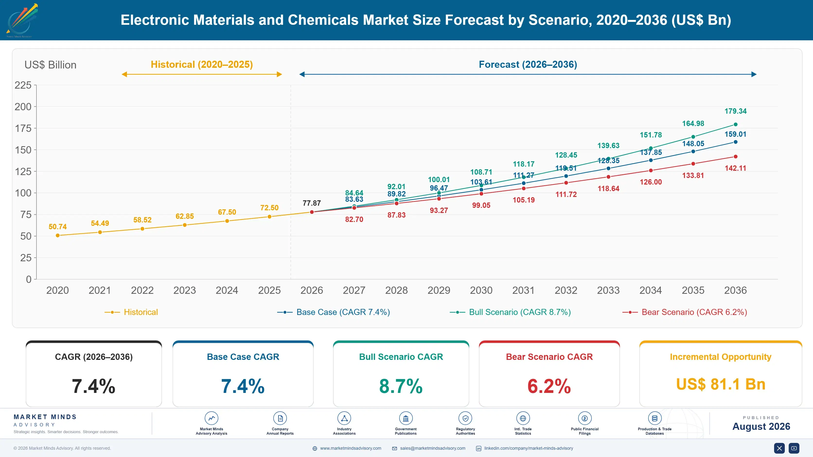
electronic-materials-and-chemicals-market-size-forecast-scenario-1787310475101
Growth of 6.1% across 2020 to 2025 concealed two violent movements pulling against each other. Pandemic device demand drove wafer starts to records through 2021 and into 2022, then memory pricing collapsed and fabs cut utilisation sharply through 2023. Underneath that cycle, leading-edge materials intensity kept rising as node transitions added process steps, which supported value even when wafer volumes fell.
The base case at 7.4% rests on three mechanisms. Subsidised fab construction across the United States, Europe, Japan and India adds wafer capacity that consumes materials regardless of who owns the fab. Process complexity keeps rising, since each node transition adds lithography, deposition and planarisation steps that raise materials cost per wafer. And advanced packaging grows faster than front-end fabrication, consuming substrate, underfill and bonding materials that traditional wafer processing never required at this scale.
The bull case at 8.7% turns on artificial intelligence accelerator demand sustaining leading-edge and advanced packaging investment beyond current plans, which would pull materials intensity up sharply. The bear case at 6.2% turns on export controls. Further restrictions on materials supply into China would fragment the market into parallel supply chains, and the duplication that follows costs considerably more than it adds in volume.

What Governs Electronic Materials Value

Aggregate concentration understates this market badly. The top five hold 34% of revenue, which looks competitive until you examine any individual material class, where two or three suppliers routinely hold most of the qualified volume. Extreme ultraviolet photoresist, certain deposition precursors and several specialty gases each come from a supply base narrow enough that a single plant outage moves the whole industry. Diversity across the aggregate hides fragility within every line of it.
TOP FIVE SHARE34%Concentration of electronic materials revenue across the largest suppliers
MATERIALS COST PER WAFERUSD 480Materials spend per twelve-inch wafer at leading process nodes
FAB QUALIFICATION CYCLE14 monthsTime from sample submission to production release at a fab
IMPURITY SPECIFICATION LEVEL1 ppbMetallic impurity ceiling that leading node materials must meet
WAFER FAB SHARE58%Front-end fabrication share of total electronic materials consumption
TOP PRODUCER SHARE42%Share of global materials output from the leading producing country
Qualification is what makes those positions durable. A fab tests a material for 14 months, correlates it against yield across thousands of wafers, then writes it into a process recipe that nobody reopens without cause. Impurity ceilings near 1 ppb mean a batch variation invisible in most chemical markets shows up as a yield excursion here.
Materials intensity rather than wafer volume drives value. Each node transition adds process steps, and materials cost per wafer near USD 480 at leading nodes runs several times what mature nodes consume. Value therefore grows even in years when wafer starts fall, which is why this market weathered the 2023 downturn far better than equipment did.
"Everybody counts fabs and nobody counts qualification slots. A fab can be built in three years and a new photoresist supplier qualified into it in fourteen months, but only if somebody started the conversation before the concrete was poured, and in most of these subsidised projects nobody did."
Director, Semiconductor Materials and Supply Chain Practice · MMA Technology / S

Market Trends

Advanced Packaging Materials Grow Faster Than Front-End

Chiplet architectures and high-bandwidth memory stacking have made packaging a performance-determining step rather than an afterthought, and the materials required differ completely from wafer fabrication. Organic substrates, underfills, thermal interface materials and hybrid bonding chemistries now account for roughly 26% of materials value against a considerably smaller share five years ago. The supplier base differs too, drawn from printed circuit board and adhesive companies rather than from wafer chemical producers, which has brought participants into semiconductor supply chains who were never previously part of them and who bring quite different commercial habits.
Market Impact: Covers 42 fabs under construction
Export Controls Fragment Supply Into Parallel Chains

Restrictions on advanced materials and equipment flowing into China have pushed both sides toward duplicated supply chains, with Chinese fabs qualifying domestic photoresist, gas and slurry suppliers while Western fabs increasingly avoid Chinese-origin inputs altogether. Roughly 31% of Chinese wafer fab materials consumption now comes from domestic suppliers, against a fraction of that before controls tightened. Duplication raises aggregate materials spending without adding wafer output, which flatters market growth figures while leaving the industry less efficient than it was before controls tightened. Neither side shows any sign of reversing course.
Market Impact: Reaches USD 480 per wafer

Market Opportunities and Growth Drivers

Subsidised Fab Construction Adds Capacity Across Four Regions

The United States CHIPS Act, European Chips Act, Japanese subsidy programmes and India's semiconductor mission have together committed public funding to wafer capacity on a scale that the industry has never before seen assembled all at once. Roughly 42 new fabs are under construction or commissioning worldwide. Each carries materials consumption from the day it starts qualification wafers, and that demand exists regardless of whether the fab ultimately proves commercially sound, which makes it unusually reliable near-term volume for whichever materials suppliers are positioned to serve it when qualification begins.
Market Impact: Qualification takes 14 months

Node Transitions Raise Materials Intensity Per Wafer

Each process node adds lithography exposures, deposition layers and planarisation steps, so a leading-edge wafer consumes materials worth roughly USD 480 against a fraction of that at mature nodes. Extreme ultraviolet lithography alone adds resist, underlayer and rinse chemistries with no equivalent in earlier generations. This decouples materials value from wafer volume in a way that protects suppliers through downturns, and it is the principal reason this market kept growing through 2023 while semiconductor equipment revenue fell sharply across the whole industry. Materials intensity is the more durable of the two drivers here.
Market Impact: Top five hold 34% aggregate

Market Restraints and Challenges

Qualification Cycles Delay Every New Supplier Entry

A fab qualifies a material across 14 months of testing, correlating it against yield on thousands of wafers before releasing it into a production recipe. The root cause is economic rather than procedural: a materials-induced yield excursion at a leading-edge fab costs far more than any conceivable saving on the material itself, so nobody accepts qualification risk. Commercially this protects incumbents and delays every subsidised localisation programme. Mitigation runs through early engagement during fab design, joint development with device makers, and acquiring suppliers who already hold qualified positions rather than building them slowly.
Market Impact: Reaches 26% of materials value

Single-Source Material Classes Create Fragile Supply Points

Aggregate concentration at 34% disguises material classes where two or three suppliers hold nearly all qualified volume. The root cause is that qualification economics reward incumbency so heavily that second sources are rarely developed until a disruption forces the issue. Commercially the exposure falls on device makers rather than on suppliers, which is a large part of why nobody has yet fixed it properly. Participants are responding with dual qualification programmes at leading fabs, regional inventory buffers measured in months, and joint development agreements that fund alternative chemistry well before it is actually needed.
Market Impact: Domestic supply reaches 31% share
4 additional market trends, 2 additional growth drivers, and 3 additional restraints and challenges are covered in the full report. Contact sales@marketmindsadvisory.com to access the complete intelligence.

Segment CAGR and Growth Architecture

Segmentation follows material class, which is the dimension determining purity requirement, qualification burden, supplier concentration and realised margin together. Process step and device type cut across most material classes without separating them commercially, since the same wet chemical serves logic and memory alike, so both belong in demand analysis rather than in this primary hierarchy.
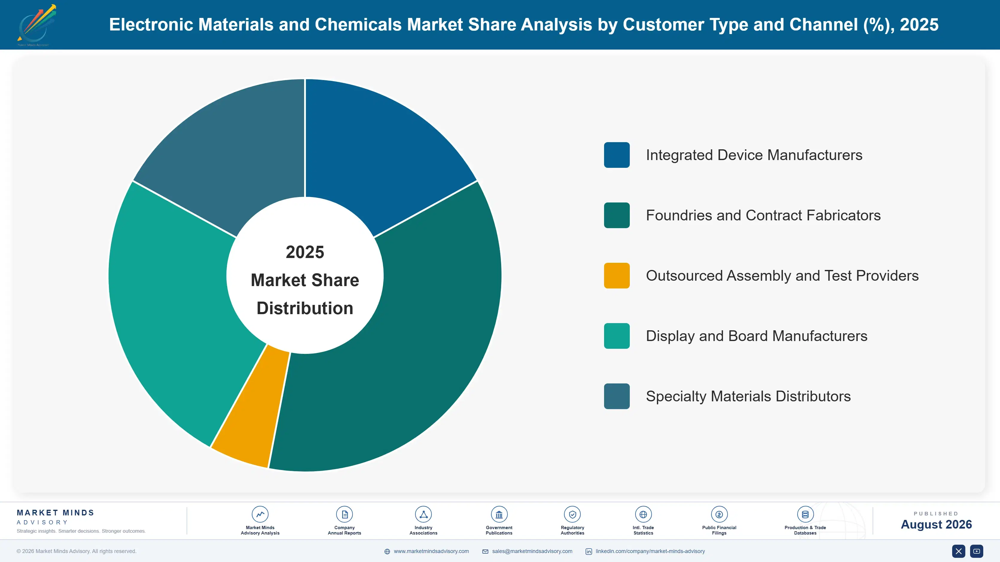
electronic-materials-and-chemicals-market-market-share-analysis-1787310475641

Photoresists and Advanced Lithography Materials

Growing at 11.1%, exactly 1.50 times the market rate, and the most concentrated part of this market by a considerable distance. Extreme ultraviolet exposure requires resist chemistries with sensitivity, resolution and line edge roughness characteristics that only a handful of Japanese suppliers have ever produced at production purity, alongside underlayers, topcoats and rinse chemistries that form a matched system rather than separate products. Each node transition adds exposures and therefore volume. Qualification is the most demanding anywhere in electronic materials, which protects incumbent positions almost absolutely and makes every localisation programme considerably harder than its government sponsors ever anticipated. Realised margins here fund a large share of the industry's development spending.
CAGR 11.1%

Electronic Specialty Gases

Expanding at 9.2% on etch, deposition and chamber cleaning demand that rises with every added process step, across a product range spanning fluorinated etchants, deposition precursors, dopants and the rare gases that excimer lasers require. Supply is unusually exposed geopolitically, as the 2022 neon disruption demonstrated when Ukrainian production halted and lithography-grade supply tightened worldwide within weeks. Purity requirements reach parts per billion and delivery infrastructure is capital intensive, since gases move through dedicated on-site systems rather than in drums. Industrial gas majors and Korean specialists dominate the qualified supply base, and regional supply is genuinely necessary rather than merely preferable, which shapes where new capacity has to be built.
CAGR 9.2%
Full segment breakdown across 6 segments available in the complete report.

Regional Architecture and Country Demand Map

Regional value follows wafer fabrication capacity and the materials supply chains that grew alongside it, which are concentrated far more tightly than semiconductor policy announcements suggest. Public funding has begun moving fabs across regions; it has moved the materials supply behind them considerably less so far.

East Asia

Fifty-five percent of value sits here, far outside the band applied to global markets. Note: the deviation is genuine rather than analytical, since leading-edge wafer fabrication and the materials supply chain serving it are concentrated in this region to a degree no other technology market approaches. Taiwan and South Korea host the majority of leading-node capacity, Japan supplies photoresists, specialty gases and deposition precursors that essentially nobody else produces at production purity, and China has built substantial mature-node capacity alongside a domestic materials base that export controls accelerated considerably. Growth of 8.2% runs above the global rate. Japanese supplier concentration remains the industry's single most consequential dependency, and no announced programme changes it soon.
Share: 55% | CAGR: 8.2% (2026 to 2036)

North America

Sixteen percent of value, below the usual band because East Asian concentration compresses every other share. CHIPS Act funding has committed substantial capacity across Arizona, Texas, Ohio and New York, and those fabs will consume materials at leading-node intensity once running. The materials supply serving them is another matter: qualification of domestic sources takes 14 months and most programmes began late, so early production will run largely on imported materials from the same Japanese and Korean suppliers the policy was partly intended to diversify away from. Growth of 8.6% is the highest outside Asia, reflecting fab commissioning rather than any expansion in domestic materials capability. Qualification programmes started late almost everywhere.
Share: 16% | CAGR: 8.6% (2026 to 2036)
Regional intelligence for 5 additional markets available in the complete report: Western Europe, South Asia and Pacific, Latin America, Middle East and Africa, Eastern Europe. Contact sales@marketmindsadvisory.com.
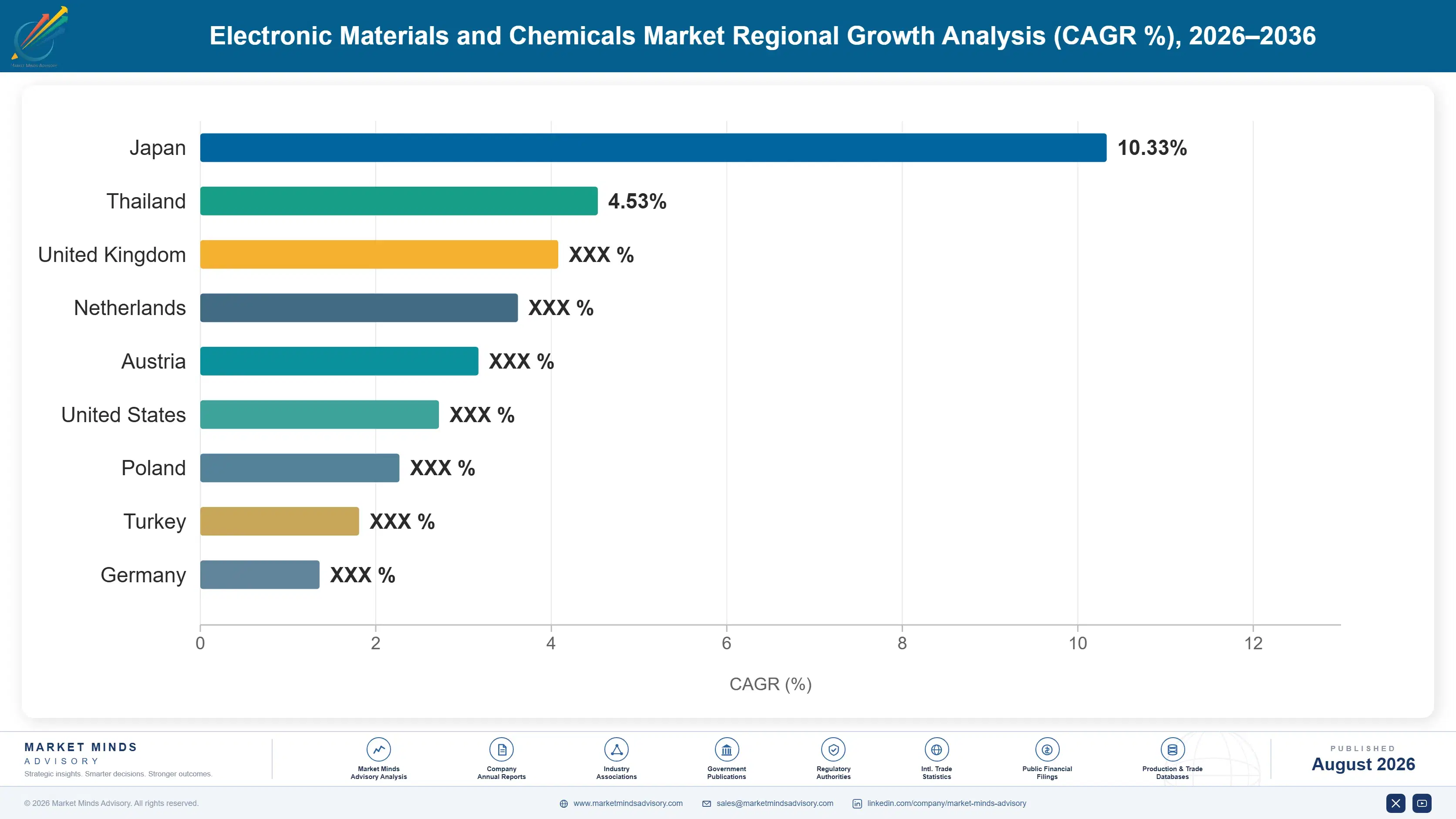
electronic-materials-and-chemicals-market-country-cagr-analysis-1787310476159

Where Materials Suppliers Can Earn More

Competing for qualified positions after a fab is running means waiting for an incumbent to fail, which is a poor commercial strategy and a slow one. The value available sits in engaging before construction, in the material classes where second sources genuinely do not exist, and in packaging chemistries growing faster than the wafers themselves.

Engage Fab Projects Before Construction Rather Than After

Qualification takes 14 months and process recipes close well before a fab reaches volume production, which means a supplier approaching a commissioning fab has already lost. Those engaging during fab design, supplying development volumes and running joint yield correlation work secure qualified positions worth roughly 55% more lifetime value per fab than late entrants achieve. The cost is technical service and sample supply rather than capital. Roughly 42 fabs are currently under construction, and most materials commercial teams are still watching for tenders that will never actually be issued to them.
Market Impact: Secures roughly 55% more lifetime v

Develop Second-Source Positions In Concentrated Material Classes

Several material classes run with two or three qualified suppliers because nobody funded an alternative until a disruption forced it, and device makers now carry that exposure knowingly. Suppliers who develop qualified second-source positions in those classes command roughly 30% above competitive material pricing, because the customer is buying supply security rather than chemistry. Device makers will co-fund the development work when asked properly, which most suppliers never do because they assume qualification is a barrier to be climbed rather than a shared problem worth solving jointly with the customer.
Market Impact: Commands roughly 30% above competit

Build Advanced Packaging Materials Capability Deliberately

Packaging now accounts for 26% of materials value and grows faster than front-end fabrication, on chemistries drawn from adhesives, substrates and thermal management rather than from wafer processing. The competitive set here is genuinely open, since traditional wafer chemical suppliers hold limited packaging capability while packaging suppliers hold limited semiconductor qualification experience. Whoever manages to bridge both capabilities earns roughly 40% above conventional packaging material margins. The capability gap is organisational rather than technical in nature, which makes it considerably faster to close than most participants assume before attempting it.
Market Impact: Earns roughly 40% above conventiona

Establish Regional Supply Where Localisation Policy Demands It

Subsidised fabs across four regions face content expectations their materials supply cannot currently meet, and the gap between announced capacity and qualified regional supply is genuine rather than rhetorical. Suppliers building regional blending, purification or fill capability ahead of that demand capture roughly 3 times the share they hold in comparable imported positions, because policy pressure and delivery logistics both favour a regional supplier decisively. The investment is modest relative to a fab's capital cost, and the window closes permanently as soon as those qualification programmes conclude and recipes are released.
Market Impact: Captures roughly 3 times comparable

Who Controls the Margin Pool

Aggregate concentration is misleading here. The top five participants hold 34% of electronic materials revenue, the basis used throughout this section, which suggests a competitive market and describes nothing anybody would recognise from inside it. Within individual material classes two or three suppliers routinely hold most qualified volume, and the gap between Shin-Etsu and the rest reflects breadth across many such positions rather than dominance in any single one.
Competition currently runs on three dimensions and unit price is the weakest. Qualification status decides who can supply a process at all, and it cannot be acquired quickly at any price. Impurity consistency decides whether a qualified position survives, since a yield excursion traced to materials ends relationships permanently. Geopolitical acceptability now decides which suppliers a fab can consider before technical evaluation begins.

Pressure is building from two directions. Chinese domestic suppliers are qualifying into domestic fabs at a pace export controls accelerated rather than slowed. Packaging materials are drawing entrants from adjacent industries with no semiconductor history. Rankings shift first in advanced packaging, where qualification norms are less established and the competitive set remains genuinely open.
electronic-materials-and-chemicals-market-company-positioning-matrix-1787310476682

Competitive Moat and Risk Dimensions

SHIN-ETSU CHEMICAL

Moat: Breadth of qualified positions

Holding qualified positions across photoresists, silicone materials, rare earth compounds and wafer products simultaneously creates a supply relationship with fabs that no single-product competitor can match, and it spreads qualification investment across a portfolio rather than a line. Decades of yield correlation data at leading customers is evidence that no entrant can assemble at any speed.
SHIN-ETSU CHEMICAL

Risk: Geographic concentration exposure

Production concentrated in Japan carries seismic, logistical and increasingly political exposure that customers are actively working to reduce, and localisation programmes across four regions are explicitly designed to diversify away from exactly this dependency. Building qualified regional capacity is expensive and slow, and moving too cautiously risks ceding subsidised fab positions permanently.
MERCK KGAA

Moat: European scale and integration

Substantial electronic materials scale built through acquisition gives breadth across lithography, deposition and specialty chemicals, with European manufacturing that suits customers seeking supply outside East Asia. Integration across materials classes allows the company to serve fab projects as a portfolio supplier rather than negotiating each material separately with different buyers.
MERCK KGAA

Risk: Leading-edge position gaps

The most demanding leading-edge positions, particularly extreme ultraviolet resist, remain with Japanese suppliers holding qualification histories built over multiple node generations. Competing there requires sustained investment against incumbents with better data and closer customer development relationships, and European energy costs pressure the more commodity end of the portfolio simultaneously.

Players Tracked

Prominent Players

Shin-Etsu Chemical
Merck KGaA
JSR Corporation
DuPont
Entegris

Other Key Players

Tokyo Ohka Kogyo
Fujifilm Holdings
Sumitomo Chemical
Resonac
Air Liquide
Linde
Air Products and Chemicals
Soulbrain
Dongjin Semichem
SK Materials
Ibiden
Shinko Electric Industries
Nitto Denko
Mitsui Chemicals
BASF

Recent Developments

MARCH 2025

Photoresist capacity commissioned outside Japan

Extreme ultraviolet and advanced immersion photoresist manufacturing capacity entered qualification testing at a manufacturing site outside Japan, addressing long-standing customer requirements for supply geography diversification following several years of pressure from device makers and their government sponsors across multiple subsidised fab programmes on three separate continents.
Signal: Moving resist production out of Japan is t
AUGUST 2025

Advanced packaging materials joint development agreement signed

A materials supplier and a device manufacturer concluded a joint development agreement covering hybrid bonding and underfill chemistries for high-bandwidth memory stacking, sharing both qualification cost and yield correlation data across a multi-year programme tied to specific packaging platform generations and their production ramp schedules.
Signal: Device makers co-funding qualification wor
NOVEMBER 2025

Domestic Chinese specialty gas qualification completed

Chinese domestic suppliers completed qualification of etch and deposition gases at mature-node fabs, displacing imported material across several distinct process steps and continuing a substitution trend that export controls accelerated considerably considerably faster than either side had originally anticipated when the restrictions were first drafted.
Signal: Controls intended to constrain capability

What Sits Inside Materials Cost

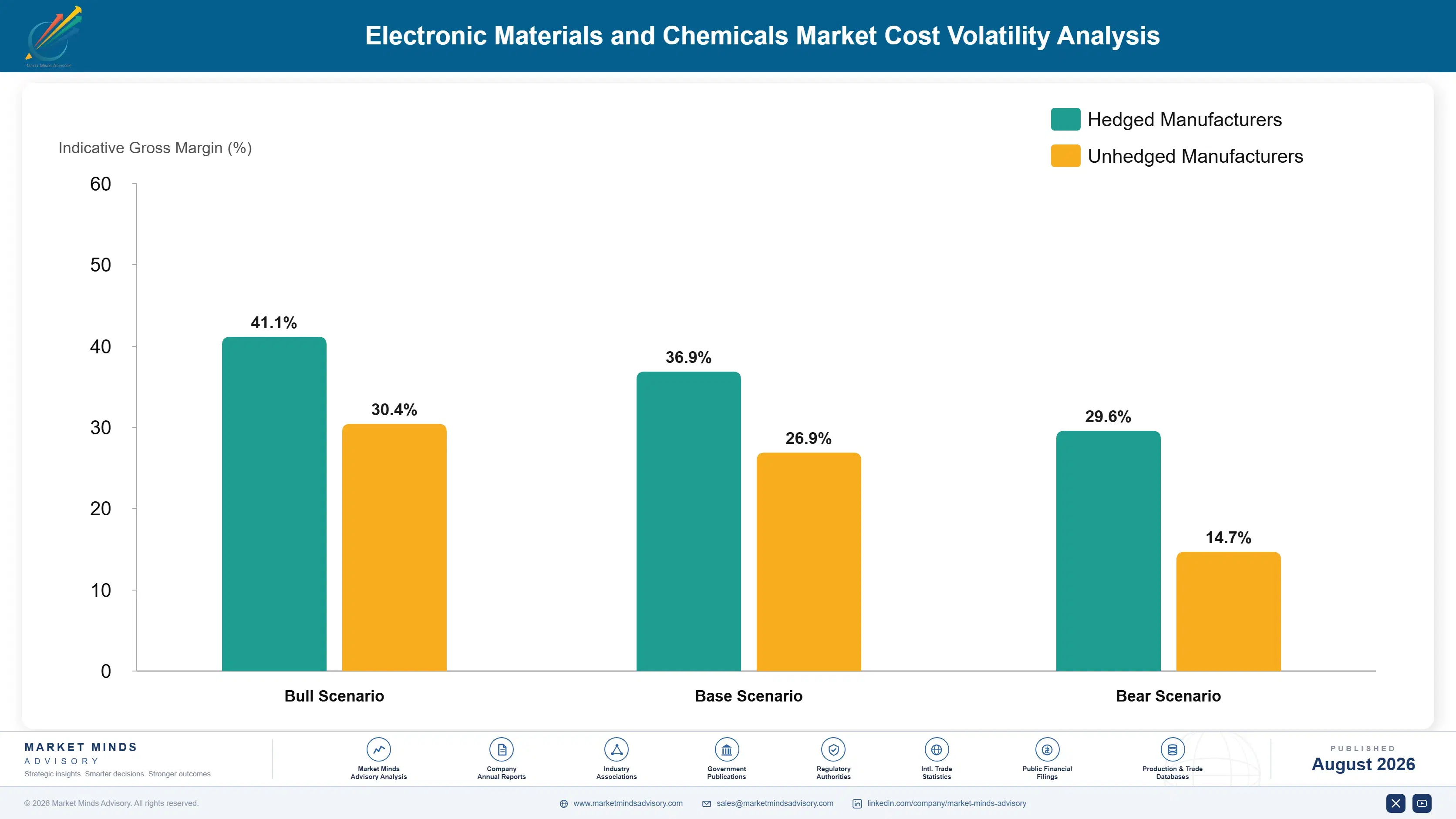
Cost structure varies enormously by material class, which makes aggregate figures less useful here than elsewhere. Specialty monomers, polymers and precursor chemicals account for roughly 38% of production cost across the portfolio, sourced from a narrow fine chemical base in Japan, Germany and increasingly China. Ultra-high purification adds around 21%, ultrapure water and energy about 12%, and specialised packaging a further 9%.
Rare gas supply proved genuinely fragile in 2022. Ukrainian neon production, which had supplied a substantial share of lithography-grade gas globally as a by-product of steel making, halted following the invasion, and excimer laser gas availability tightened worldwide within weeks. Linde Annual Report 2022 and Air Liquide Annual Report 2022 both recorded the disruption and the subsequent investment in alternative capacity, alongside European energy costs that raised purification expense over the same period.

The competitive disadvantage mechanism runs through purification capability rather than raw material access. Meeting parts-per-billion metallic impurity ceilings requires purification trains, cleanroom handling and analytical capability that general chemical production never involves, and that capital sits idle if qualification fails. Established suppliers amortise it across many qualified positions. New entrants carry the full cost against one uncertain programme, which is why so few persist.
electronic-materials-and-chemicals-market-cost-volatility-analysis-1787310476879

Qualify alternative precursor sources before disruption arrives

Fine chemical precursors frequently come from a single supplier because nobody examined the dependency until it failed, and requalifying a precursor means requalifying the material at every fab consuming it. Mapping the supply chain two tiers back and qualifying alternatives in advance costs far less than the disruption it prevents, and considerably less than requalifying under pressure.

Amortise purification capital across multiple qualified positions

Purification and analytical infrastructure is expensive to build and largely shared across material classes, so a supplier holding several qualified positions carries a permanent advantage over one attempting a single programme. That arithmetic favours portfolio breadth over narrow specialisation, which is precisely the opposite of what most entrants assume when they first plan their entry.

Contract rare gas supply across multiple producing regions

The 2022 neon disruption demonstrated that by-product gas supply concentrated in one country is a fragile arrangement whatever the commercial terms attached to it. Contracts spanning several producing regions cost more in normal conditions and cost far less than a lithography halt, which is a calculation that remarkably few buyers had bothered to make beforehand.

Portfolio Architecture for Margin Defence

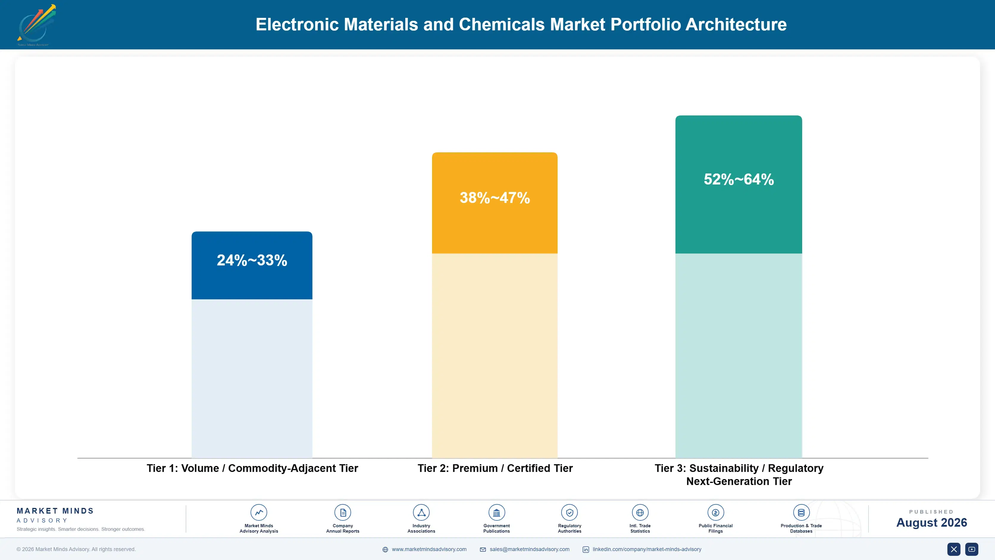
Margin architecture here separates by qualification difficulty rather than by chemistry sophistication. Wet process chemicals and commodity cleaning agents earn what regional supply and purity capability allow, which is respectable and not remarkable, because qualification is achievable and second sources exist. Value rises steeply where qualification is punishing and alternatives do not exist, which describes lithography materials and several deposition precursors almost exactly.
The volume versus premium tension is unusual because volume and premium sit in different fabs. Mature-node capacity consumes large quantities of comparatively straightforward chemicals at prices reflecting genuine competition. Leading-edge capacity consumes smaller volumes of materials nobody else can supply, at margins that fund the entire industry's development spending. A supplier serving only mature nodes has scale without pricing power, and one serving only leading edge has pricing power on volumes too small to build a business.

High-value pools concentrate in three places. Extreme ultraviolet lithography materials command price because the qualified supplier list is barely longer than one entry in several categories. Advanced packaging chemistries earn well because demand is growing faster than qualified capability. And regional supply into subsidised fabs earns a premium that policy rather than chemistry creates.

Volume / Commodity-Adjacent Tier

Wet process chemicals, cleaning agents and bulk gases supplied into mature-node fabrication and printed circuit board manufacture, where purity requirements are achievable, second sources exist and regional competition determines pricing directly.
Gross Margin: 24-33%

Premium / Certified Tier

Chemical mechanical planarisation slurries, sputtering targets, packaging substrates and deposition materials qualified at production fabs. Qualification history and impurity consistency defend pricing. The nine-point range reflects mature against leading-node qualified positions.
Gross Margin: 38-47%

Sustainability / Regulatory / Next-Generation Tier

Extreme ultraviolet photoresists, advanced lithography ancillaries and hybrid bonding chemistries where qualified supply is extremely narrow. Scarcity and qualification difficulty defend pricing almost absolutely. The twelve-point range reflects established against emerging platform positions.
Gross Margin: 52-64%
electronic-materials-and-chemicals-market-portfolio-architecture-1787310477384

High-value Sub-segments and Strategic Watch-out

Extreme ultraviolet lithography material systems

High value and high growth together, because resist, underlayer, topcoat and rinse form a matched system that only a handful of suppliers have produced at production purity, and every node transition adds exposures. Qualification difficulty here protects incumbent positions more completely than anywhere else in electronic materials.
Gross Margin: 52-64%

Advanced packaging and hybrid bonding chemistries

Strong realised value on the fastest packaging growth, because chiplet architectures and memory stacking have made these materials performance-determining rather than incidental. The competitive set remains genuinely open, since wafer chemical suppliers and adhesive companies each hold only half of the capability actually required here.
Gross Margin: 42-55%

Wet process chemicals and cleaning agents

The volume core, consumed heavily across mature-node fabrication and board manufacture while earning only what regional competition and achievable purity requirements will permit. Necessary for scale and customer breadth, but this tier will never fund leading-edge development work on its own terms or its own margins.
Gross Margin: 24-33%

Regional supply into subsidised fab programmes

The strategic watch-out, because roughly 42 fabs under construction face content expectations their materials supply cannot presently meet, and qualification windows close permanently the moment process recipes are released. Suppliers building regional capability late will find those positions already taken by whoever moved first on them.
Gross Margin: 36-50%

How Materials Demand Behaves

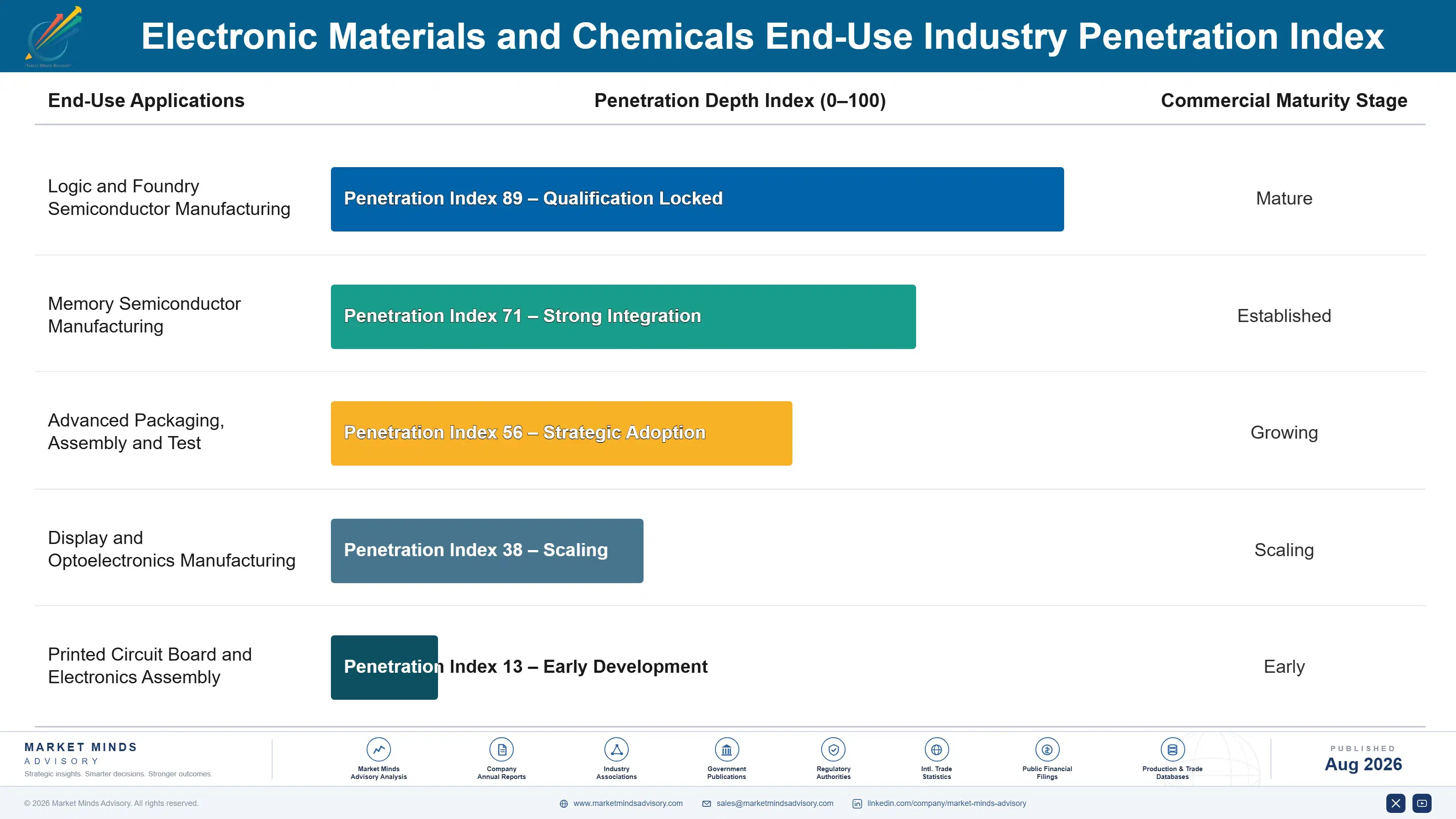
Demand is recipe-locked annuity revenue attached to running process tools. A material qualified into a process recipe is consumed at a fixed rate per wafer for the life of that process, reordered against fab loading, and displaced only when the node retires or something goes wrong. Winning that position takes 14 months of qualification and considerable technical service; holding it costs almost nothing. That asymmetry explains why suppliers defend qualified positions so fiercely.
Stickiness varies sharply with process criticality. Bulk chemicals and cleaning agents are loosest, retendered against specification where several qualified suppliers exist and switching means only a modest requalification. Planarisation slurries and deposition precursors sit considerably tighter, because performance interacts with process tuning in ways that make substitution genuinely risky. Lithography materials are stickiest of all, where changing resist means requalifying an entire exposure process.

The buyer profile has shifted toward supply chain and government affairs in a way the industry finds uncomfortable. A decade ago process engineers selected materials on performance and procurement negotiated the price. Today geographic origin, export control exposure and content requirements shape the candidate list before technical evaluation begins, which advantages suppliers whose footprint matches policy rather than whose chemistry performs best.
electronic-materials-and-chemicals-market-end-use-penetration-index-1787310477876

Where We Land On This

These are among the four positions where our research anticipates prominent divergence between winners and laggards over the coming forecast period. Each is grounded in the demand model, the regulatory perimeter, and the announced capacity pipeline.
01 / PRE-CONSTRUCTION FAB ENGAGEMENT

Engage fab projects during design, not at commissioning

Qualification runs 14 months and process recipes close well before a fab reaches volume production, so a supplier approaching a commissioning fab is competing for positions that have already been decided elsewhere. Those engaging during fab design and running joint yield correlation work secure qualified positions worth roughly 55% more lifetime value per fab than any late entrant achieves. Roughly 42 fabs are currently under construction, and most materials organisations are still waiting patiently for tenders that nobody intends to issue.
02 / SECOND-SOURCE POSITION DEVELOPMENT

Build alternatives in the concentrated classes customers fear

Several material classes operate with two or three qualified suppliers because nobody funded an alternative until a disruption forced the question, and device makers now carry that exposure with full knowledge of it. Suppliers developing qualified second-source positions command roughly 30% above competitive material pricing, because the customer is buying supply security rather than performance. Device makers will co-fund the development work when properly asked, which suppliers rarely do because they mistake qualification for a barrier rather than a shared commercial problem.
03 / PACKAGING CAPABILITY BUILDING

Bridge wafer chemistry and packaging materials capability

Advanced packaging accounts for 26% of materials value and grows faster than front-end fabrication, on chemistries drawn from adhesives, substrates and thermal management rather than from anything in conventional wafer processing. Wafer chemical suppliers hold semiconductor qualification experience without any packaging capability, while packaging suppliers hold precisely the reverse, so whoever bridges both earns roughly 40% above conventional packaging margins. The gap is organisational rather than technical in nature, which makes closing it considerably faster than most participants assume before they attempt it.
04 / POLICY-ALIGNED REGIONAL FOOTPRINT

Place regional capacity before qualification windows close

Subsidised fabs across four regions face content expectations that their current materials supply cannot meet, and the gap between announced wafer capacity and qualified regional supply is genuine rather than rhetorical posturing. Suppliers building regional blending, purification or fill capability ahead of that demand capture roughly 3 times the share they hold in comparable imported positions. The window closes permanently once qualification programmes conclude, and no amount of later investment reopens a process recipe once it has been released to production.

Engagement Snapshot From the Field

A live engagement with an industry participant carrying material or product regulatory and market exposure ahead of a defining policy shift, showing how our research translates into a defensible multi-year portfolio strategy.
MARKET MINDS ADVISORY · CLIENT ENGAGEMENT SUMMARY
Electronic Materials and Chemicals Producer Strategic Portfolio Review and Transition Roadmap 2026·Investment Scenario on Electronic Materials and Chemicals Exposure Evaluation 2025-26
CLIENT PROFILE
A specialty chemical producer with established fine chemical and purification operations across Europe and North America, supplying pharmaceutical and industrial customers, and holding a small electronic materials business selling wet process chemicals into mature-node fabrication. Electronic materials revenue approached USD 95 million annually (client-reported, unverified by MMA), entirely in commodity-adjacent chemistries with no leading-node qualified position anywhere.
STRATEGIC CHALLENGE
Management intended to expand into higher-value semiconductor materials on the back of announced regional fab construction, and had budgeted a purification capacity investment. Two earlier attempts to qualify at leading fabs had failed without any clear explanation reaching the commercial organisation. Nobody had established which material classes were genuinely open and which were closed by qualification history.
MMA APPROACH
MMA interviewed forty-seven fab process engineers, materials qualification leads, supply chain directors and competing suppliers across five markets, reconstructing how qualification decisions are actually reached and when. We mapped qualification timelines against construction schedules at every announced regional fab, assessed the client's purification and analytical capability against leading-node requirements, and reviewed both failed submissions in detail.
KEY FINDINGS
  1. Both failed qualifications had been rejected on analytical capability rather than material performance, because the client could not demonstrate parts-per-billion metallic measurement in its own laboratory to the fab's satisfaction.
  2. Every regional fab the client hoped to supply had begun materials qualification eighteen months or more before commissioning, and recipe positions for four of six target material classes were already effectively closed.
  3. Advanced packaging chemistries showed a genuinely open competitive set where the client's adhesive and formulation capability transferred directly, and where no supplier held an entrenched qualification history.
  4. Purification capital would have been idle for roughly three years given qualification timelines (client-reported, unverified by MMA), while analytical capability could be built within months at a fraction of the cost.
CLIENT PROFILE
A specialty chemical producer with established fine chemical and purification operations across Europe and North America, supplying pharmaceutical and industrial customers, and holding a small electronic materials business selling wet process chemicals into mature-node fabrication. Electronic materials revenue approached USD 95 million annually (client-reported, unverified by MMA), entirely in commodity-adjacent chemistries with no leading-node qualified position anywhere.
STRATEGIC CHALLENGE
Management intended to expand into higher-value semiconductor materials on the back of announced regional fab construction, and had budgeted a purification capacity investment. Two earlier attempts to qualify at leading fabs had failed without any clear explanation reaching the commercial organisation. Nobody had established which material classes were genuinely open and which were closed by qualification history.
MMA APPROACH
MMA interviewed forty-seven fab process engineers, materials qualification leads, supply chain directors and competing suppliers across five markets, reconstructing how qualification decisions are actually reached and when. We mapped qualification timelines against construction schedules at every announced regional fab, assessed the client's purification and analytical capability against leading-node requirements, and reviewed both failed submissions in detail.
KEY FINDINGS
  1. Both failed qualifications had been rejected on analytical capability rather than material performance, because the client could not demonstrate parts-per-billion metallic measurement in its own laboratory to the fab's satisfaction.
  2. Every regional fab the client hoped to supply had begun materials qualification eighteen months or more before commissioning, and recipe positions for four of six target material classes were already effectively closed.
  3. Advanced packaging chemistries showed a genuinely open competitive set where the client's adhesive and formulation capability transferred directly, and where no supplier held an entrenched qualification history.
  4. Purification capital would have been idle for roughly three years given qualification timelines (client-reported, unverified by MMA), while analytical capability could be built within months at a fraction of the cost.
RECOMMENDED STRATEGY
Phase 1: Phase 1 (0 to 9 months): Defer the purification investment and build parts-per-billion analytical capability with fab-recognised methods and documentation. Phase 2: Phase 2 (9 to 24 months): Redirect entry toward advanced packaging chemistries where the competitive set is open, and engage two fab projects at design stage. Phase 3: Phase 3 (24 to 42 months): Pursue leading-node qualification selectively where analytical credibility and packaging relationships have been established first.
OUTCOME
The client deferred roughly USD 60 million of purification capital (client-reported, unverified by MMA) and built analytical capability for a fraction of that. Two advanced packaging development agreements were signed within eighteen months, one regional fab engagement began at design stage, and the first leading-node qualification submission was accepted for testing rather than rejected outright.

Frequently Asked Questions

Foundational context covering the market sizes, CAGR, scope, country, region and competition that inform every finding below. This section is provided to cover basics and most often pre-purchase conversations, answered from the MMA Primary Research Dataset.

What is the current size of the Electronic Materials and Chemicals Market?

The market reached USD 72.5 billion in 2025, measured as materials revenue at realised delivered price. Front-end wafer fabrication accounts for 58% of total consumption across all regions.

How large will the Electronic Materials and Chemicals Market be by 2036?

MMA forecasts USD 159.01 billion by 2036, an expansion of 2.04 times the 2026 level. Incremental value across the forecast period reaches USD 81.14 billion.

What is the CAGR for the Electronic Materials and Chemicals Market 2026 to 2036?

The base case compound annual growth rate is 7.4%, with a bull case of 8.7% and a bear case of 6.2%. Artificial intelligence demand and export control severity separate those scenarios.

Which segment is growing fastest?

Photoresists and advanced lithography materials grow fastest at 11.1%, exactly 1.50 times the overall market rate. Extreme ultraviolet exposure adds resist, underlayer and rinse chemistries with no earlier equivalent.

Who are the major companies in the Electronic Materials and Chemicals Market?

Shin-Etsu Chemical, Merck KGaA, JSR Corporation, DuPont and Entegris lead, holding 34% of revenue between them. Concentration within individual material classes runs far higher than that aggregate suggests.

Which country is growing fastest?

India grows fastest at 10.2%, where the semiconductor mission has funded assembly, test and fabrication projects carrying materials demand from first qualification wafers. Domestic chemical capability gives regional supply a genuine starting point.

Report Segmentation Architecture

The full report scope spans multiple orthogonal segmentation dimensions, with cross-tabulated demand data provided for each dimension pair. Coverage extends further to regional breakdowns, trend trajectories, and the competitive detail needed to support segment-level decision-making.

By Material Class

  • Photoresists and Advanced Lithography Materials
  • Electronic Specialty Gases
  • Advanced Packaging and Substrate Materials
  • Chemical Mechanical Planarisation Slurries and Pads
  • Sputtering Targets and Deposition Materials
  • Wet Process Chemicals

By End-Use Industry

  • Logic and Foundry Semiconductor Manufacturing
  • Memory Semiconductor Manufacturing
  • Advanced Packaging, Assembly and Test
  • Display and Optoelectronics Manufacturing
  • Printed Circuit Board and Electronics Assembly

By Customer Type and Channel

  • Integrated Device Manufacturers
  • Foundries and Contract Fabricators
  • Outsourced Assembly and Test Providers
  • Display and Board Manufacturers
  • Specialty Materials Distributors

By Region

  • North America
  • Western Europe
  • East Asia
  • South Asia and Pacific
  • Latin America
  • Middle East and Africa
  • Eastern Europe

Scope, Methodology, and Coverage

Every figure in this report is reproducible from documented input assumptions. The scope below maps the historical period, the forecast horizon, the segmentation dimensions, and the countries covered, alongside the underlying primary and qualitative methodology.
Historical Period
2020 to 2025
Forecast Period
2026 to 2036
Base Year
2025 (USD billions; MMA Primary Research Dataset, August 2026)
Market Definition
The market comprises materials and chemicals consumed directly in semiconductor and electronic device manufacturing, spanning photoresists and advanced lithography materials, electronic specialty gases, advanced packaging and substrate materials, chemical mechanical planarisation slurries and pads, sputtering targets and deposition materials, and wet process chemicals. Sizing captures materials revenue at realised delivered price across front-end wafer fabrication, advanced packaging, assembly and test, display manufacture and printed circuit board production, including captive materials production valued at transfer price. Silicon wafers, process and metrology equipment, photomasks, finished semiconductor devices, electronic manufacturing services and facility construction fall outside scope.
Quantitative Units
USD billions (current prices); materials consumption per twelve-inch wafer equivalent; USD per wafer at leading and mature process nodes
Segmentation Dimensions
By Material Class; By End-Use Industry; By Customer Type and Channel; By Region
Regions Covered
North America, Western Europe, East Asia, South Asia and Pacific, Latin America, Middle East and Africa, Eastern Europe
Countries Covered
USA, Canada, Mexico, Germany, France, Netherlands, Belgium, Ireland, UK, Italy, Poland, Czech Republic, Hungary, Israel, Taiwan, South Korea, Japan, China, Singapore, Malaysia, India, Vietnam, Thailand, Philippines, Australia, Brazil, Saudi Arabia, UAE, and additional markets relevant to this sector
Key Companies Profiled
Shin-Etsu Chemical, Merck KGaA, JSR Corporation, DuPont, Entegris, Tokyo Ohka Kogyo, Fujifilm Holdings, Sumitomo Chemical, Resonac, Air Liquide, Linde, Air Products and Chemicals, Soulbrain, Dongjin Semichem, SK Materials, Ibiden, Shinko Electric Industries, Nitto Denko, Mitsui Chemicals, BASF.
Quantitative Methodology
Primary survey, n=3,800 respondents, Q4 2025, six countries; demand-side model with trade association cross-validation
Qualitative Methodology
47 expert interviews, Q4 2025; applied to validate demand model assumptions, identify emerging dynamics, and assess competitive positioning
Report Format
PDF and XLSX data workbook (Word format preview document)
Publisher
Market Minds Advisory
Report Code
MMA-2026-TEC-452
Published
August 2026
Contact
sales@marketmindsadvisory.com | www.marketmindsadvisory.com

Purchase the full Electronic Materials and Chemicals Market Report (2026 to 2036).

The full report sizes the electronic materials and chemicals market across six material classes, five end-use industries, five customer channels and seven regions, with annual forecasts to 2036 in revenue and consumption per wafer equivalent. It maps qualification timelines against construction schedules at every announced fab, which is the analysis that establishes which supply positions remain open and which have already closed. Twenty participants are assessed on a consistent materials revenue basis, with qualified positions mapped material class by material class rather than in aggregate. Supply concentration is quantified within each class separately.
Six material classes sized and forecast annually
Qualification timelines mapped against announced fab schedules
Twenty participants on consistent materials revenue basis
Qualified positions mapped by material class individually
Supply concentration quantified within each class separately
Export control exposure assessed supplier by supplier

Built For The People Who Decide

From boardroom strategy to bench-side execution, this report is read cover-to-cover by leaders shaping the next decade of their industry, turning demand scenarios, market dynamics and valuation benchmarks into decisions.
CXOs/ Presidents/ VPs/ Managers
M&A and Corporate Development
Strategy Teams and R&D Heads
Procurement and Product Directors
Regulatory and Compliance Leaders
Investor Relations and Equity Analysts