Semiconductor Inspection Drives Metrology Volume Growth
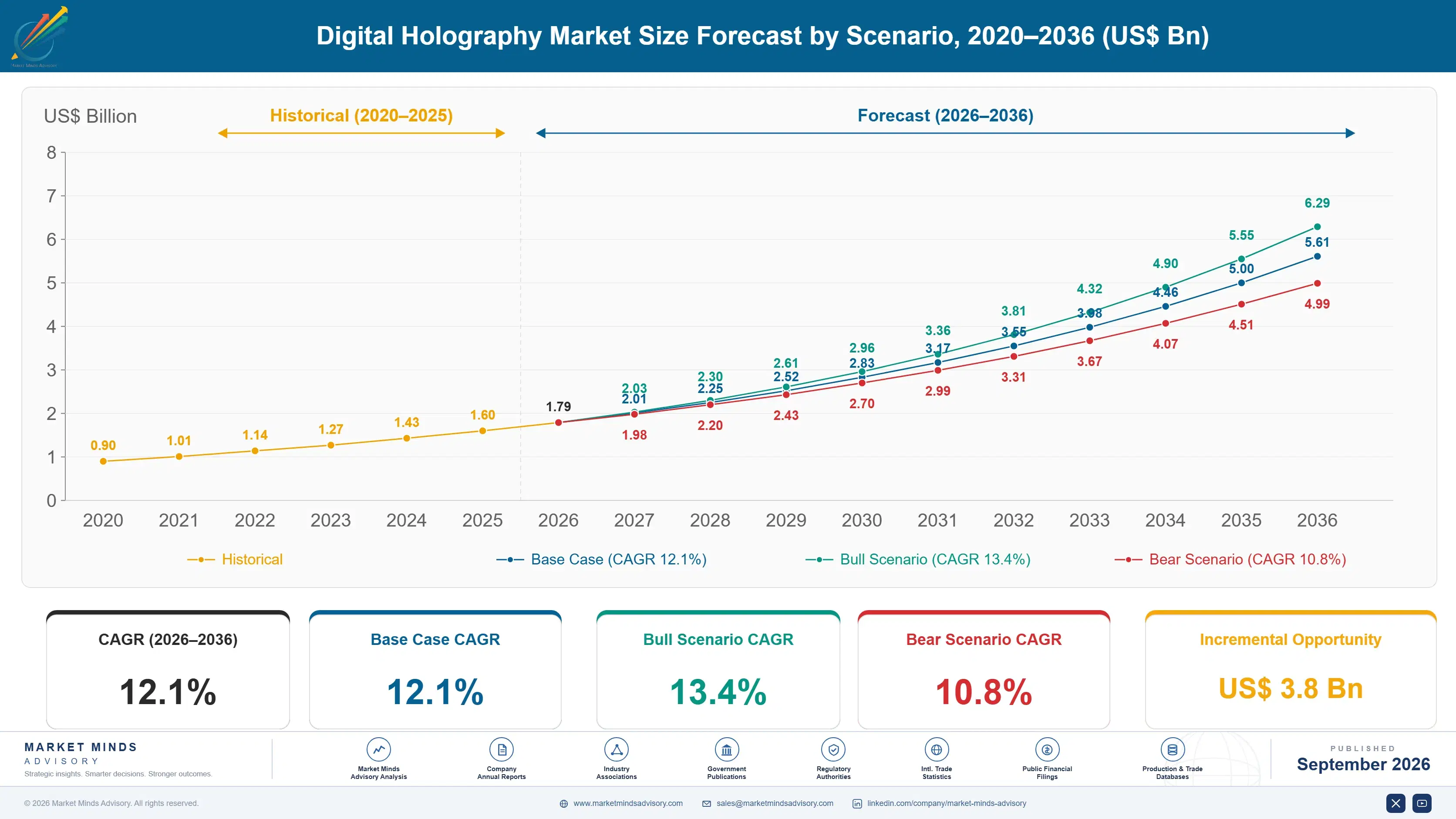
Shrinking feature sizes and increasingly three-dimensional device structures raise inspection demand for techniques that capture depth alongside surface detail in a single exposure. A tool reconstructing 400 microns of depth without mechanical focusing inspects considerably faster than anything scanning through the same range. Holographic metrology and surface inspection systems grow at 18.2% against 12.1% for the market. South Korea compounds at 19.4%, ahead of every other market, on semiconductor inspection capacity being installed right now across both memory and logic production lines. Depth capture rather than resolution is what sells here.
Market Impact: Compute carries 31% of cost