Market Minds Advisory
Chemical Vapor Deposition (CVD) Market

Chemical Vapor Deposition (CVD) Market: The Layer Nobody Sees And Everybody Depends On

Every advanced logic and memory device now depends on films a few atoms thick that cannot be deposited any other way. Precursor chemistry, not the reactor, decides who wins these tool sockets.

Lead Analyst

David Horsley

Published

September 2026

Make Smarter Decisions with Customized Research Insights

Request a free sample report and evaluate market opportunities, growth trends, and competitive dynamics relevant to your business needs.

2025 MARKET VALUE$32.8BMarket Size 2025
2036 FORECAST VALUE$84.6BBase Case , 2026 to 2036
CAGR 2026 TO 20369.0 %Bull 10.3% / Bear 7.8%
INCREMENTAL OPPORTUNITY$48.9BNet 10- year value creation
EXPANSION MULTIPLE2.37x2036 value over 2026 base
Strategic Levers
M&A Pipeline
Regional Outlook
Country Rankings
Competitive Intelligence
Segmental Deep-dive
Call-Us : 91 93563 13602

Executive Snapshot and Market Trajectory

Transistors stopped being flat around 2012 and memory stopped being flat around 2016, and neither change was possible without depositing films conformally into structures a few nanometres wide. That single requirement created this entire market. It reaches USD 32.8 billion in 2025 and compounds at 9.0% through 2036.
Atomic layer deposition grows fastest at 13.5%, exactly 1.50 times the market rate, because gate-all-around transistors and 300-layer memory stacks need the kind of thickness control that no other method can deliver. East Asia holds 44% of value, far above the band this framework applies, because essentially all leading-edge logic and memory fabrication capacity sits in Taiwan, South Korea, China, and Japan. North America follows at 22% and is now gaining share.
Concentration is high at 61% across the top five, and it holds because a deposition tool qualified into a production process is almost never displaced before the node ends. Competition happens at process development, two or three years before any revenue arrives. The precursor chemistry matters at least as much as the reactor does, and that is where the genuinely interesting margin has quietly moved.
Market Definition
The chemical vapor deposition market covers equipment and precursor chemicals used to deposit thin solid films from gaseous precursors, spanning thermal and low pressure CVD, plasma enhanced CVD, metal organic CVD, atomic layer deposition, and high-throughput industrial and optical coating systems. Physical vapor deposition, epitaxial silicon reactors, etch and cleaning equipment, wet deposition, and finished coated substrates are excluded.
Base Year Value
$32.8B in 2025 (MMA Primary Research Dataset, August 2026)
Forecast Period
2026 to 2036, eleven discrete annual values
CAGR
9.0% base case. Bull 10.3%. Bear 7.8%.
Fastest Growth Segment
Atomic Layer Deposition Systems: 13.5% CAGR
Fastest Growth Country
India: 14.2% CAGR
Fastest Growth Region
South Asia and Pacific: 11.0% CAGR
Largest Region
East Asia: 44% of 2025 global value
Market Leaders
Applied Materials, Lam Research, ASM International, Tokyo Electron, Kokusai Electric. Source: MMA Primary Research Dataset, July 2026.
Primary Survey
n=3,800 procurement and R&D decision-makers, Q4 2025, six countries
Methodology
Demand-side build-up, cross-validated against public data, 47 expert interviews

Chemical Vapor Deposition (CVD) Market Forecast Scenarios

chemical-vapor-deposition-cvd-market-size-forecast-scenario-1787333595178
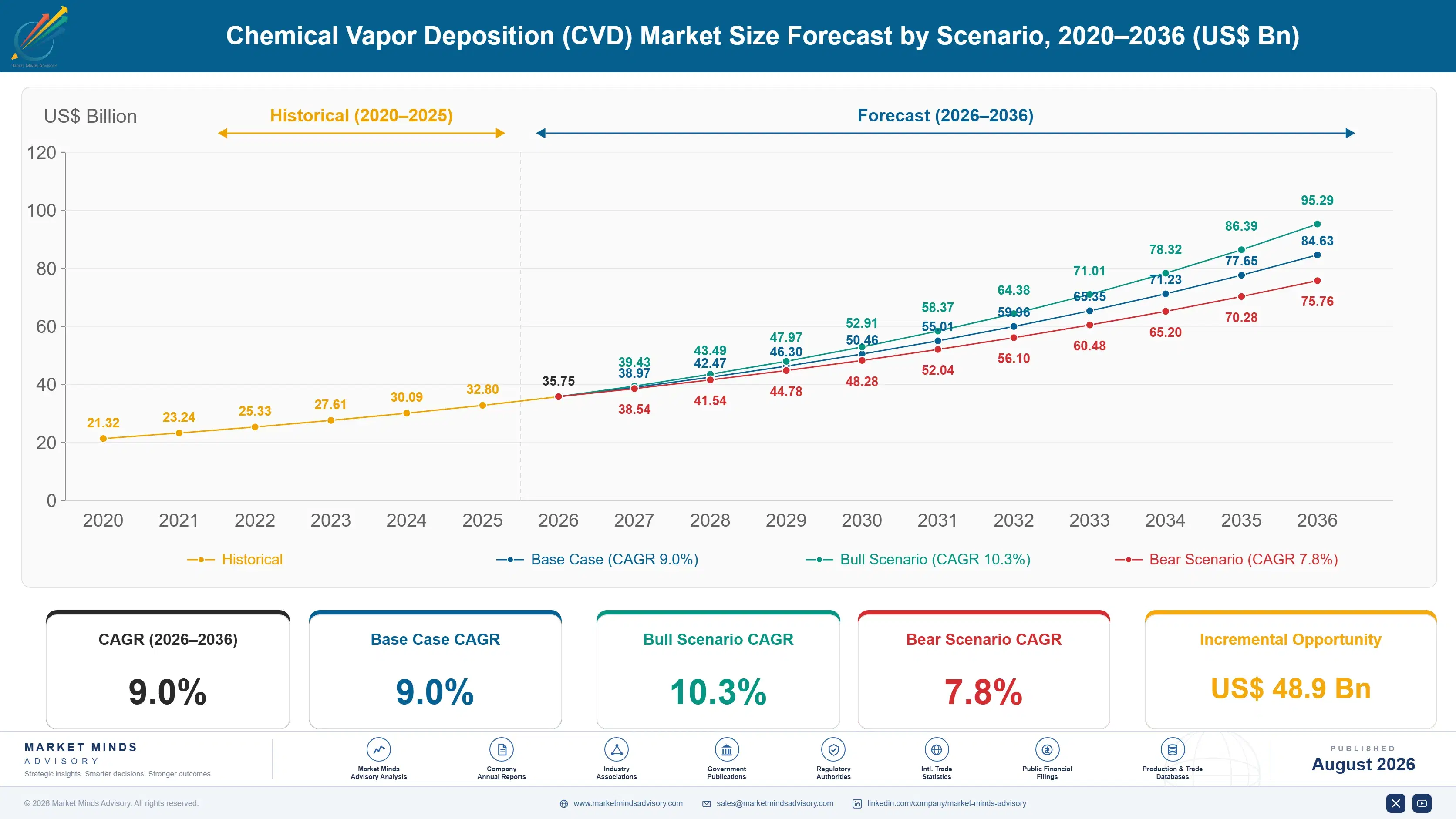
The five years to 2025 contained a boom, a correction, and a policy shock. Pandemic-era electronics demand pushed capital equipment spending to records through 2022, memory oversupply cut it hard in 2023, and export controls on advanced tooling into China reshaped who could buy what from whom. An 8.0% historical CAGR averages across all of that. It describes almost none of the individual years accurately.
Three mechanisms carry the 9.0% base case. Gate-all-around transistor architectures are the largest, since each device requires substantially more deposition steps than the finFET generation it replaces. Memory layer counts are the second, because every additional tier in a 3D NAND stack adds deposition passes and the layer race is not slowing. And government-funded capacity, through the CHIPS Act, European Chips Act, and equivalent Asian programmes, is committing fab construction independent of near-term demand.
The 10.3% bull case rests on advanced packaging, where deposition steps are multiplying as chiplet integration moves from niche to standard. The 7.8% bear case is a memory downturn of the kind that arrived in 2023, since memory makers cut equipment spending faster and deeper than logic producers and they represent a substantial share of deposition tool demand.

Films A Few Atoms Thick, Deposited Perfectly

Deposition is the quiet half of semiconductor manufacturing. Lithography gets the attention and the headlines, and it defines where features go. Deposition decides what those features are made of and whether the material actually reaches the bottom of a hole with an aspect ratio above fifty to one. On a modern logic flow there are roughly 110 deposition steps, and each one must work every time.
TOP FIVE CONCENTRATION61%Process qualification locks incumbents into production tools for years
AVERAGE SYSTEM PRICEUSD 4.2 millionTypical configured deposition platform for advanced semiconductor fabrication
PRECURSOR COST SHARE22%Chemical consumables as a portion of total ownership cost
DEPOSITION STEPS PER WAFER110Approximate count on a leading logic process flow today
TOOL QUALIFICATION TIME12 to 24 monthsDevelopment effort before a platform reaches volume production release
INSTALLED BASE SERVICE SHARE36%Portion of supplier revenue from parts, upgrades, and support
Atomic layer deposition changed the economics. By building films one atomic layer at a time through self-limiting surface reactions, it delivers conformality and thickness control that conventional CVD cannot approach. It is also slow and expensive per wafer, which is why nobody used it until device geometries left no alternative. Now it is unavoidable, and the tools that do it well command prices that reflect that.
The chemistry has become the harder problem. A reactor is engineering; a precursor that decomposes cleanly at the right temperature, deposits the intended metal, and leaves no carbon behind is chemistry that takes years to develop. Suppliers who control both the tool and the precursor have a position that reactor builders alone cannot match.
"The tool companies will tell you the reactor is the hard part. Ask a process engineer what actually keeps them awake and you will hear about precursor purity and lot-to-lot variation. That is where the next competitive shift comes from."
Director, Semiconductor Equipment Practice · MMA Technology Practice &midd

Market Trends

Gate-All-Around Architectures Multiply Deposition Step Counts

Moving from finFET to gate-all-around nanosheet transistors requires depositing and then selectively removing sacrificial layers, wrapping gate dielectric and metal around every channel, and doing all of it with atomic precision. TSMC, Samsung, and Intel have all committed to the architecture at their leading nodes, and the deposition step count rises materially against the generation it replaces. Atomic layer deposition carries most of that increase because nothing else deposits conformally into the released channel geometry. The transition is committed rather than speculative, which makes it the most reliable demand mechanism in the market.
Market Impact: CHIPS Act commits 52 billion dollar

Precursor Chemistry Becomes The Competitive Battleground

A deposition process is only as good as the molecule feeding it, and precursor development now takes considerably longer than reactor development does. New metals entering the process flow, ruthenium and molybdenum for interconnects among them, need precursors that decompose cleanly at temperatures the device can survive and leave no contamination behind. Chemical suppliers who co-develop with tool vendors capture position that pure reactor builders cannot reach. Precursors already represent roughly 22% of ownership cost, and that share rises as film stacks grow more complex and more metals enter the flow.
Market Impact: NAND exceeds 300 layers today

Market Opportunities and Growth Drivers

Government Fab Programmes Commit Capacity Regardless Of Cycle

The CHIPS Act in the United States, the European Chips Act, and equivalent Japanese, Korean, and Indian programmes have committed public money to fab construction on a scale this industry has not seen before. Those projects proceed on political timelines rather than on demand signals, which decouples a meaningful slice of equipment demand from the semiconductor cycle that normally governs it. Deposition tools represent a substantial share of every fab's equipment budget. For suppliers, this is order visibility extending years further out than commercial fab planning ever provided. Very little else in this business offers anything comparable.
Market Impact: Controls affect 30% of China demand

Memory Layer Counts Keep Rising Without An Obvious Ceiling

3D NAND has passed 300 layers in production and roadmaps point considerably higher, with each additional tier requiring deposition passes into holes whose aspect ratios already exceed anything else in manufacturing. DRAM capacitor structures face the same problem from a different direction entirely. Samsung, SK Hynix, Micron, Kioxia, and YMTC are all committed to the layer race because it is the only remaining route to cost per bit reduction now that lateral scaling has stopped. Every layer added is deposition equipment and precursor volume that did not previously exist. The roadmaps published so far show no ceiling at all.
Market Impact: Qualification takes 24 months minim

Market Restraints and Challenges

Export Controls Fragment The Largest Growth Market

Restrictions on advanced deposition tooling into China have removed a substantial revenue stream for American, Japanese, and Dutch suppliers, and the controls keep tightening rather than easing. The root cause is that deposition equipment is dual-use by nature: the same tool that makes a memory chip makes an advanced logic device. Commercially it splits the market into served and unservable segments and accelerates Chinese domestic tool development that will eventually compete elsewhere. Suppliers are mitigating by expanding mature-node offerings that remain permitted and by shifting capacity toward compliant regions and customers.
Market Impact: Adds 25 deposition steps per wafer

Qualification Cycles Lock Out New Entrants For Years

A deposition tool qualified into a production process is not replaced until the next node, and qualification itself takes twelve to twenty-four months of joint development before any revenue arrives. The root cause is risk: a fab running billions of dollars of wafers will not experiment with an unproven deposition step. Commercially this cements incumbency, holds concentration at 61%, and makes challenger economics brutal since the investment precedes revenue by years. Newer entrants are mitigating by targeting emerging materials where no incumbent has an entrenched process, and by partnering with research consortia.
Market Impact: Precursors reach 22% of ownership c
4 additional market trends, 3 additional growth drivers, and 2 additional restraints and challenges are covered in the full report. Contact sales@marketmindsadvisory.com to access the complete intelligence.

Segment CAGR and Growth Architecture

Segmentation follows deposition process, meaning the physical mechanism by which the film is actually formed, because that single choice determines film quality, throughput, achievable geometry, and which device structures the tool can serve in volume production. Precursor revenue is attributed to the process it feeds rather than being treated as a dimension of its own.
chemical-vapor-deposition-cvd-market-market-share-analysis-1787333595722

Atomic Layer Deposition

Atomic layer deposition grows fastest at 13.5%, exactly 1.50 times the market rate, and it grows because device geometry left the industry no alternative. Self-limiting surface reactions build film one atomic layer at a time, which delivers conformality into structures with aspect ratios above fifty to one and thickness control measured in single atoms. Gate-all-around transistors and 300-layer memory stacks cannot be built without it. Throughput is poor and cost per wafer is high, and neither matters when the alternative is a device that does not work. ASM International holds the strongest position here, and the precursor chemistry attached to each process is where much of the value now sits.
CAGR 13.5%

Plasma Enhanced CVD

Plasma enhanced CVD grows at 8.8%, using plasma energy to drive deposition at temperatures the underlying device can tolerate. That thermal budget advantage makes it the workhorse for dielectric films, hard masks, and the barrier and passivation layers that every process flow needs in real quantity. Volume is high and the step count rises with device complexity even where atomic precision is entirely unnecessary. Advanced packaging has become an important secondary driver, since chiplet integration requires dielectric and barrier films across interposers and redistribution layers. Applied Materials and Lam Research dominate the segment, and displacement partway through a node is rare enough to be genuinely notable. Throughput economics keep it viable where atomic layer deposition would be unaffordable.
CAGR 8.8%
Full segment breakdown across 7 segments available in the complete report.

Regional Architecture and Country Demand Map

Regional shares here track where wafers are actually processed, not where chips are designed or ultimately consumed. Semiconductor fabrication capacity is geographically concentrated to a degree almost no other industry matches, and policy funding is now shifting that map for the first time in decades.

East Asia

East Asia takes 44% of value against a 30% ceiling in this framework, and the concentration of wafer fabrication capacity explains all of it. Taiwan hosts the majority of leading-edge foundry output, South Korea holds the bulk of global memory production, and both buy deposition tooling on a scale that nothing else anywhere approaches. Chinese fabs are investing heavily in mature-node capacity while domestic tool builders work to replace equipment that export controls have put out of reach. Japanese fabs are smaller consumers, but Japanese suppliers hold strong positions in both tooling and precursor chemistry. Growth at 9.6% exceeds the global rate on continued leading-edge and memory capacity additions. Suppliers benefit from proximity to the customers setting the roadmap.
Share: 44% | CAGR: 9.6% (2026 to 2036)

North America

North America holds 22% of value and is gaining share for the first time in roughly three decades. CHIPS Act funding has committed fab construction in Arizona, Ohio, Texas, and New York that would never have been economic on purely commercial terms, and those projects proceed on political timelines rather than on demand signals. Intel, TSMC, Samsung, and Micron all have American capacity under construction or already ramping. The region also hosts Applied Materials and Lam Research, which shapes how tool development priorities get set globally. Growth at 9.4% sits close to the global rate, front-loaded into the construction phase of the funded projects. Advanced packaging investment adds a second demand stream alongside front-end capacity.
Share: 22% | CAGR: 9.4% (2026 to 2036)
Regional intelligence for 5 additional markets available in the complete report: Western Europe, South Asia and Pacific, Latin America, Middle East and Africa, Eastern Europe. Contact sales@marketmindsadvisory.com.
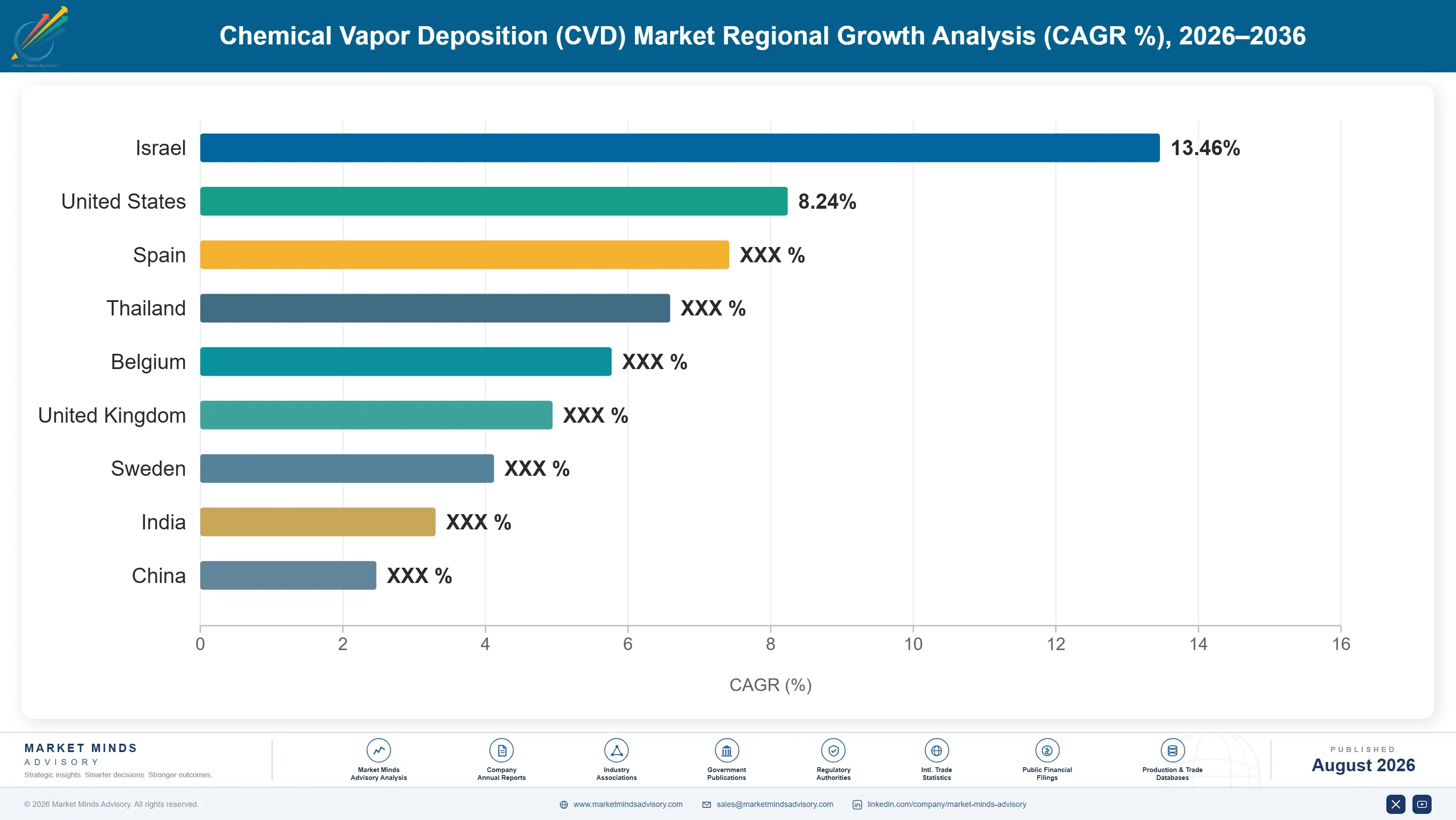
chemical-vapor-deposition-cvd-market-country-cagr-analysis-1787333596257

Where Deposition Margin Actually Sits

Margin in deposition does not sit in shipping reactors. It sits in owning the precursor that feeds the process, in the parts and upgrade revenue that follows every tool for a decade after installation, and in getting into process development early enough that the customer's specification gets written around your platform. The reactor itself is the least defensible part.

Own The Precursor Attached To Every Process

Precursor chemicals already represent roughly 22% of ownership cost and they recur for the entire life of the tool, unlike the reactor which sells exactly once. Suppliers controlling both the platform and the molecule capture a revenue stream running 15% to 20% of installed tool value annually, at gross margins above the equipment itself. Co-development also locks the process, because requalifying a different precursor means revalidating the film properties. Reactor builders without chemistry capability watch that recurring value flow to Merck, Air Liquide, and Entegris instead of collecting it. Chemistry capability is not something a reactor builder acquires quickly.
Market Impact: Precursors yield 15 to 20 percent o

Get Into Process Development Before The Node Freezes

Tool selection happens two to three years before high-volume production, during joint development at the customer's pilot line, and the platform that proves the process usually holds the socket for the node's full life. Winning at that stage costs applications engineering and dedicated development tools with no immediate revenue attached, and it returns 200 to 400 million dollars of orders across a successful node ramp. Suppliers who treat development engagement as a cost centre rather than as the actual sales process consistently lose sockets they could have held. The economics of that trade are not close.
Market Impact: Node sockets return 200 to 400 mill

Grow Service And Upgrade Revenue On Installed Tools

A deposition platform runs ten to fifteen years and consumes chamber parts, kits, and process upgrades throughout that life, and installed base revenue already accounts for around 36% of supplier turnover. It is also counter-cyclical, holding up when new tool orders collapse in a downturn as they did through 2023. Node extension upgrades that let a customer run a newer process on existing hardware are the highest-margin item in the whole category. Suppliers underinvesting in service organisations discover the gap only when the cycle turns against them. By then the cycle has already done its damage.
Market Impact: Installed base carries 36% of total

Who Controls the Margin Pool

Concentration reaches 61% across the top five, measured on deposition equipment and precursor revenue, and it holds because a tool qualified into a production process is rarely displaced before the next node. Applied Materials leads on breadth across CVD and packaging deposition, while ASM International holds the strongest atomic layer deposition position and the fastest-growing book. Lam Research, Tokyo Electron, and Kokusai Electric follow. The gap to the next tier is process qualification dep
Competition currently plays out at three points. Joint development engagement two to three years before production, where sockets are actually won. Precursor and chemistry co-development, which increasingly decides whether a process works at all. And installed base service, which carries revenue through the downturns that periodically flatten new tool orders. Price rarely decides anything at the leading edge.

Pressure is coming from Chinese domestic tool builders, whom export controls have handed a protected home market and considerable state funding. NAURA, AMEC, and Piotech are closing the gap on mature-node deposition faster than most Western suppliers expected. Rankings will shift first in China and mature-node segments elsewhere, and only much later, if at all, at the leading edge.
chemical-vapor-deposition-cvd-market-company-positioning-matrix-1787333596787

Competitive Moat and Risk Dimensions

APPLIED MATERIALS

Moat: Breadth across every deposition process

Applied Materials supplies CVD, ALD, epitaxy, and packaging deposition from one portfolio, which lets a fab source most of its deposition requirement from a single vendor with one applications organisation behind it. That breadth compounds during joint development, because a supplier already embedded on five process steps gets consulted on the sixth before anyone else does.
APPLIED MATERIALS

Risk: China revenue exposure under controls

A substantial share of revenue came from Chinese customers before export controls arrived, and those restrictions keep tightening rather than easing. The lost revenue is only part of it: the controls are actively funding a domestic competitor base that will eventually compete outside China, which turns a near-term revenue problem into a longer-term competitive one.
ASM INTERNATIONAL

Moat: Atomic layer deposition process leadership

ASM holds the strongest position in the fastest-growing deposition method, built through decades of ALD process development and reinforced by early engagement on gate-all-around transistor programmes. Because ALD is where the difficult films now sit, that leadership converts directly into sockets on the nodes that matter, and displacing it means requalifying the most sensitive steps in the flow.
ASM INTERNATIONAL

Risk: Narrower portfolio than competitors

ASM's concentration in ALD is its strength and its exposure, since a customer sourcing most deposition from a broader vendor has an obvious consolidation argument available whenever commercial pressure builds. Competitors with wider portfolios can bundle across process steps in a way ASM cannot answer, and ALD leadership has to be re-earned at every node.

Players Tracked

Prominent Players

Applied Materials
ASM International
Lam Research
Tokyo Electron
Kokusai Electric

Other Key Players

Veeco Instruments
Aixtron
Jusung Engineering
Wonik IPS
Eugene Technology
NAURA Technology
Advanced Micro-Fabrication Equipment
Piotech
CVD Equipment Corporation
Oxford Instruments
Beneq
Entegris
Merck KGaA
Air Liquide
Adeka Corporation

Recent Developments

JANUARY 2025

Leading foundry selected ALD platforms for gate-all-around production

A leading foundry completed tool selection for its gate-all-around node, awarding atomic layer deposition sockets for the sacrificial layer and gate stack steps. Selection followed roughly two years of joint development at the pilot line, which is where these decisions are actually made rather than in procurement.
Signal: Sockets are effectively decided during joi
OCTOBER 2024

Chemical supplier and tool vendor co-developed molybdenum precursor

A precursor supplier and an equipment vendor jointly released a molybdenum precursor qualified for interconnect deposition, addressing the resistivity limits that copper now runs into at advanced nodes. The chemistry took considerably longer to develop than the deposition hardware it feeds ever did. That inversion is recent.
Signal: Precursor development timelines now gate n
MAY 2025

Chinese tool builder shipped domestic PECVD into mature-node fab

A Chinese equipment manufacturer shipped domestically developed plasma enhanced CVD platforms into a mature-node fab, replacing tooling that export controls had made unavailable to the customer. The installation is a qualification milestone rather than a commercial one, and it establishes a production reference the supplier previously lacked.
Signal: Export controls are producing exactly the

Precision Components, Chemistry, And Power

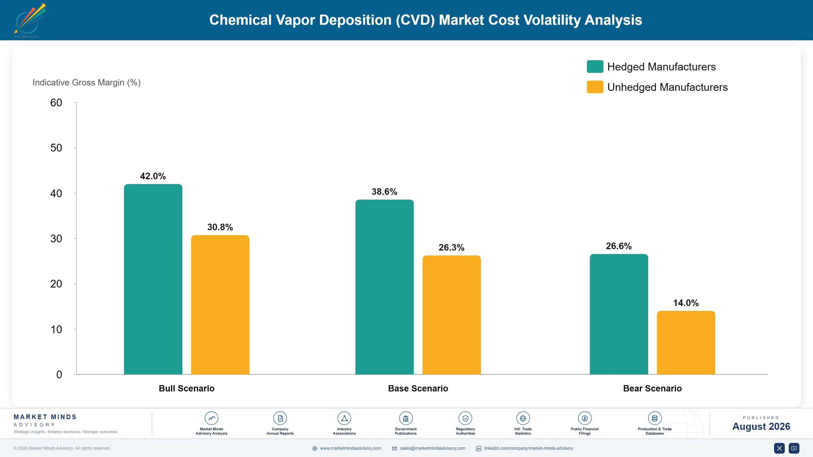
Precision machined chambers, vacuum components, and mass flow controllers carry roughly 34% to 42% of cost of goods, sourced from a narrow supplier base concentrated in the United States, Japan, and Germany. Specialty gases and precursor chemicals add 18% to 24% and depend on Japanese, Korean, and European chemical producers. Power supplies, RF generators, and control electronics make up most of the remainder.
Neon supply for the wider specialty gas chain came under severe pressure in 2022 when Ukrainian production, which supplied a large share of semiconductor-grade neon, stopped. Prices rose by multiples and fabs drew down inventory while alternative capacity qualified. Air Liquide and Linde both documented specialty gas disruption in their 2022 reporting, and the episode exposed how narrow the qualified supply base for semiconductor-grade materials actually is.

Exposure varies by where a supplier sits in the chain. Tool builders pass component cost into system pricing across long order lead times and feel it slowly. Precursor and gas suppliers face it immediately and cannot always pass it through, since fab supply agreements often fix prices annually. Smaller specialty chemical producers without qualified second sources sit worst, because a single plant outage removes their ability to supply at all.
chemical-vapor-deposition-cvd-market-cost-volatility-analysis-1787333596992

Qualify second sources for every critical precursor

Semiconductor-grade materials require full customer qualification, so a second source has to be approved before it is needed rather than found during a disruption. Running dual qualification on every critical precursor costs test wafers and engineering time upfront, and it removes the single-plant exposure that the 2022 gas episode made visible across the industry.

Index gas and chemical contracts to feedstock benchmarks

Annual fixed-price supply agreements leave chemical producers absorbing feedstock and energy movement entirely, which is unsustainable through the kind of shock that followed 2022. Indexing the raw material portion to published benchmarks shares the volatility with fabs that can absorb it more easily, and it removes the risk premium suppliers would otherwise build into base pricing.

Design components toward available machining capacity

Precision chamber and vacuum components come from a narrow qualified machining base, and designs specifying unusual tolerances or materials narrow it further without much benefit. Design rules that target broadly available capacity shorten lead times and widen the supplier field. The trade-off is engineering flexibility, which teams surrender reluctantly and only under sustained delivery pressure.

Portfolio Architecture for Margin Defence

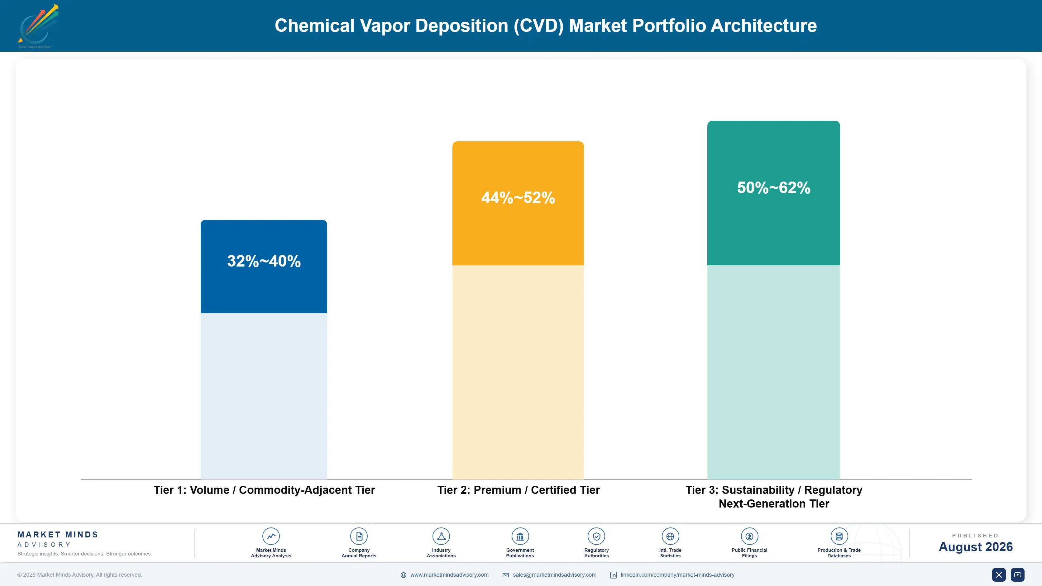
Margin here tracks process criticality rather than tool complexity. Mature-node dielectric deposition is competitive and increasingly contested by Chinese suppliers, and the pricing reflects that clearly. Atomic layer deposition on leading-edge logic and memory sits behind a qualification barrier and a process knowledge gap that very few suppliers clear at all, and it prices as the genuinely scarce capability it is.
The volume tension runs between cyclical tool revenue and steady consumables. New system sales are large, lumpy, and collapse during downturns, which is what happened through 2023. Precursor and service revenue is smaller per transaction, recurring, and holds up when capital spending stops. Suppliers weighted entirely toward equipment discover the difference painfully every cycle, and most rediscover it each time.

High-value pools sit in three places. Atomic layer deposition for gate-all-around and high layer count memory, precursor chemistry for the newer metals entering the interconnect flow, and node extension upgrades sold into the installed base. All three are protected by qualification rather than by patents, which is a considerably more durable barrier because it costs the customer time as well as money to cross.

Volume / Commodity-Adjacent Tier

Mature-node dielectric and passivation deposition platforms, industrial and optical coating systems, and standard chamber consumables. The range reflects how differently Chinese and established suppliers price into a market where the process is well understood.
Gross Margin: 32-40%

Premium / Certified Tier

Advanced logic and memory deposition platforms qualified into production flows, plus the applications support attached to them. Qualification depth rather than hardware cost supports the margin, since displacement mid-node is effectively impossible for a customer.
Gross Margin: 44-52%

Sustainability / Regulatory / Next-Generation Tier

Atomic layer deposition for gate-all-around and high layer count memory, novel metal precursors, and node extension upgrades. The wide range reflects genuinely different economics between hardware, chemistry, and software-enabled upgrades sold into installed tools.
Gross Margin: 50-62%
chemical-vapor-deposition-cvd-market-portfolio-architecture-1787333597500

High-value Sub-segments and Strategic Watch-out

Atomic Layer Deposition for Advanced Logic

Growing at 13.5% and the highest margin position available anywhere in this market, because gate-all-around transistors cannot be built without it and the qualified supplier field is very narrow. Process knowledge accumulated over years, rather than hardware capability, is what defends the position. Hardware alone gets nobody in.
Gross Margin: 52-64%

Precursor Chemistry for New Metals

Growing quickly as ruthenium and molybdenum enter interconnect flows, carrying recurring revenue for the full operating life of every tool. Development timelines now run longer than reactor engineering does, which limits how fast any competitor can respond once a molecule is qualified into a process.
Gross Margin: 46-58%

Mature-Node Dielectric Deposition

The volume base of the equipment market, increasingly contested by Chinese suppliers operating behind export controls with substantial state funding behind them. It funds applications organisations and service networks, and remains defensible mainly on installed base relationships rather than on technology. Pricing has already begun to erode steadily.
Gross Margin: 32-40%

Advanced Packaging Deposition

Growing fast as chiplet integration moves from niche to standard, requiring dielectric and barrier films across interposers and redistribution layers. The watch-out is that packaging fabs buy on cost far more readily than front-end fabs do, which caps how far pricing can realistically hold. Volume growth is real regardless.
Gross Margin: 38-50%

What Follows The Tool Order

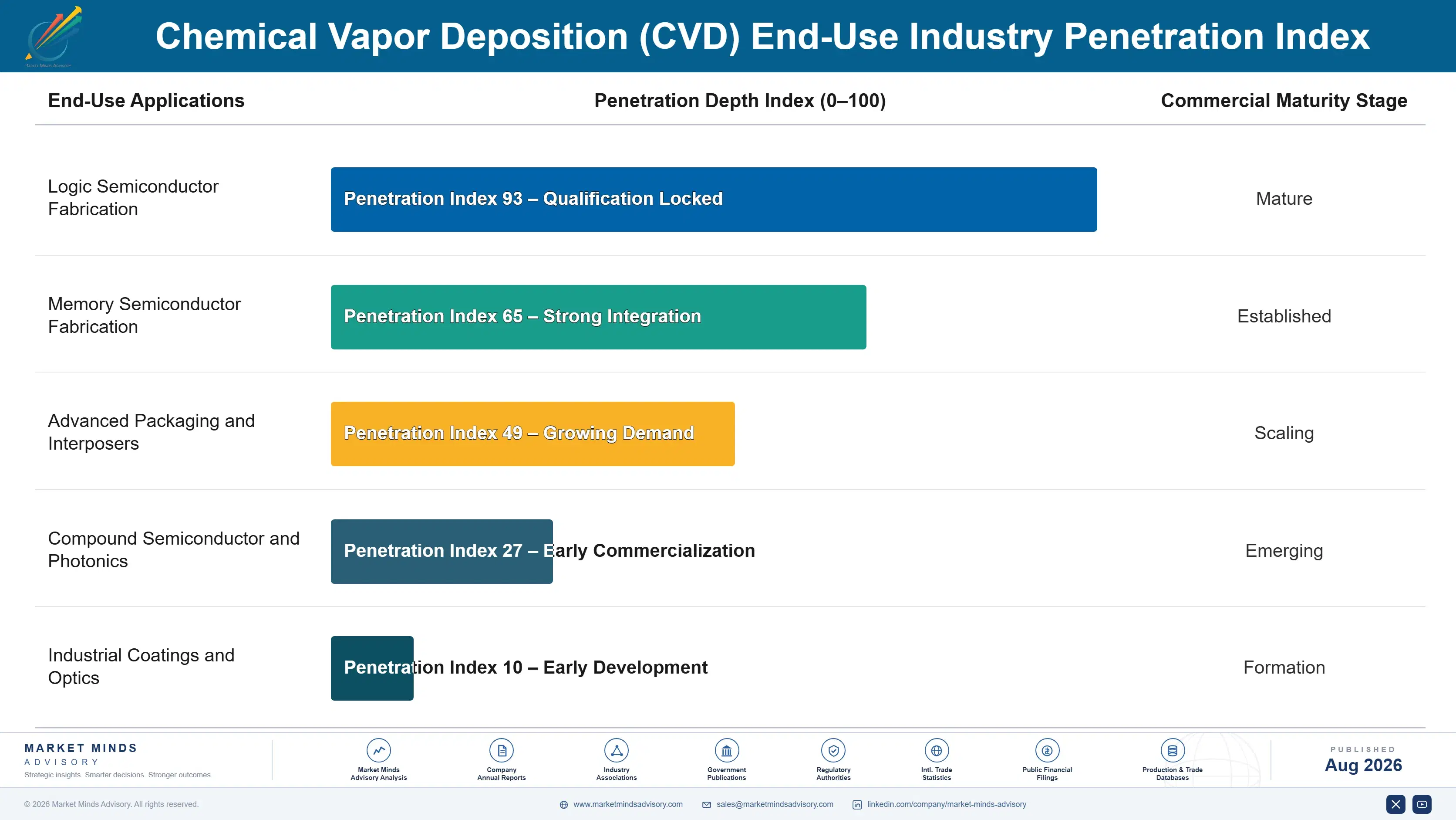
Deposition equipment generates annuity income that rivals the original sale. A platform runs ten to fifteen years, consuming chamber kits, precursor chemistry, and process upgrades throughout, and installed base revenue already carries roughly 36% of supplier turnover. It is also counter-cyclical, holding steady through the downturns that periodically halve new tool orders, which is why suppliers with deep service organisations survive cycles that damage their competitors.
Stickiness varies enormously by customer type and node. Leading-edge logic and memory fabs are locked in for a node's full life, because requalifying a deposition step means revalidating film properties across an entire process flow that nobody will risk. Mature-node fabs have more freedom and increasingly use it, particularly in China. Research institutions and packaging houses switch most readily, since their processes are not frozen into high-volume production.

Buying behaviour has moved earlier and deeper into engineering. Tool selection now happens during joint development at pilot lines two to three years before production, with process integration engineers rather than procurement making the effective decision. Suppliers organised around competitive bidding are arriving after the choice has been made, which is why applications engineering headcount predicts socket wins better than pricing strategy ever has.
chemical-vapor-deposition-cvd-market-end-use-penetration-index-1787333597991

Where To Compete Here

These are among the four positions where our research anticipates prominent divergence between winners and laggards over the coming forecast period. Each is grounded in the demand model, the regulatory perimeter, and the announced capacity pipeline.
01 / PRECURSOR CHEMISTRY OWNERSHIP

Own the molecule, not only the reactor

Precursors already carry roughly 22% of ownership cost and they recur for the full life of every tool, while the reactor itself sells exactly once and then stops earning. Suppliers controlling both the platform and the chemistry collect a recurring stream at margins above the equipment, and they lock the process, because requalifying a molecule means revalidating the film. Reactor builders without any chemistry capability of their own are simply handing that recurring value to Merck, Air Liquide, and Entegris year after year.
02 / DEVELOPMENT STAGE ENGAGEMENT

Win the socket during development, not procurement

Tool selection happens two to three years before high-volume production, at the customer's pilot line, and the platform that first proves the process usually holds the socket for the node's entire commercial life. That means applications engineering headcount is the real sales force here, whatever the organisation chart happens to say about it. Suppliers who treat development engagement as a cost centre rather than as the actual selling process go on losing sockets they were perfectly capable of holding onto.
03 / INSTALLED BASE MONETISATION

Service revenue is what survives the downturn

Installed base parts, kits, and upgrades already carry around 36% of supplier revenue and they hold up when new tool orders collapse, exactly as they did across the 2023 downturn. Node extension upgrades letting a customer run a newer process on existing hardware are the highest-margin item in the whole category by some distance. Suppliers underinvesting in their service organisations only discover the gap once the cycle turns against them, by which point building one properly takes far too long.
04 / CHINA STRATEGY CLARITY

Decide what the China business actually is

Export controls have split this market into served and unservable segments, and they keep tightening rather than easing on any realistic planning timeline that anyone can point to today. The controls are also funding a domestic competitor base that will eventually compete outside China, which turns today's revenue problem into tomorrow's competitive one. Suppliers need an explicit board-level position on mature-node participation rather than a quiet hope that the restrictions ease, because planning on the latter has consistently failed everyone.

Engagement Snapshot From the Field

A live engagement with an industry participant carrying material or product regulatory and market exposure ahead of a defining policy shift, showing how our research translates into a defensible multi-year portfolio strategy.
MARKET MINDS ADVISORY · CLIENT ENGAGEMENT SUMMARY
Chemical Vapor Deposition (CVD) Producer Strategic Portfolio Review and Transition Roadmap 2026·Investment Scenario on Chemical Vapor Deposition (CVD) Exposure Evaluation 2025-26
CLIENT PROFILE
A mid-sized deposition equipment supplier with roughly USD 1.1 billion in annual revenue (client-reported, unverified by MMA), holding strong positions in mature-node dielectric platforms and a smaller atomic layer deposition business. Around a third of revenue had historically come from Chinese customers, and export controls had removed a significant portion of that within eighteen months.
STRATEGIC CHALLENGE
The board needed to decide whether to defend mature-node share against rapidly improving Chinese competitors, or redirect development spending toward atomic layer deposition where the client held credible technology but almost no leading-edge process qualifications. Both paths were affordable; doing both properly was not, and the engineering organisation was already stretched.
MMA APPROACH
MMA modelled socket availability by node and process step across the client's addressable customers through 2032, mapping which sockets came up for selection and when. Chinese competitor capability was assessed step by step rather than in aggregate. Precursor supply relationships were examined to identify where chemistry partnership could substitute for scale the client did not have.
KEY FINDINGS
  1. Mature-node dielectric sockets facing Chinese competition showed pricing erosion of 9% annually (client-reported, unverified by MMA), with no evident floor as domestic capability improved.
  2. Only eleven atomic layer deposition sockets across the client's addressable customers would open for selection before 2030, making timing far more decisive than technology readiness.
  3. The client's ALD technology tested competitively on two specific film types but lacked the applications engineering depth to support pilot line engagement at more than three customers simultaneously.
  4. Precursor co-development with a specialty chemical partner could substitute for roughly half the applications resource gap at considerably lower cost than hiring.
CLIENT PROFILE
A mid-sized deposition equipment supplier with roughly USD 1.1 billion in annual revenue (client-reported, unverified by MMA), holding strong positions in mature-node dielectric platforms and a smaller atomic layer deposition business. Around a third of revenue had historically come from Chinese customers, and export controls had removed a significant portion of that within eighteen months.
STRATEGIC CHALLENGE
The board needed to decide whether to defend mature-node share against rapidly improving Chinese competitors, or redirect development spending toward atomic layer deposition where the client held credible technology but almost no leading-edge process qualifications. Both paths were affordable; doing both properly was not, and the engineering organisation was already stretched.
MMA APPROACH
MMA modelled socket availability by node and process step across the client's addressable customers through 2032, mapping which sockets came up for selection and when. Chinese competitor capability was assessed step by step rather than in aggregate. Precursor supply relationships were examined to identify where chemistry partnership could substitute for scale the client did not have.
KEY FINDINGS
  1. Mature-node dielectric sockets facing Chinese competition showed pricing erosion of 9% annually (client-reported, unverified by MMA), with no evident floor as domestic capability improved.
  2. Only eleven atomic layer deposition sockets across the client's addressable customers would open for selection before 2030, making timing far more decisive than technology readiness.
  3. The client's ALD technology tested competitively on two specific film types but lacked the applications engineering depth to support pilot line engagement at more than three customers simultaneously.
  4. Precursor co-development with a specialty chemical partner could substitute for roughly half the applications resource gap at considerably lower cost than hiring.
RECOMMENDED STRATEGY
Phase 1: Phase one: concentrate atomic layer deposition development on the two film types where testing showed genuine competitive advantage rather than pursuing breadth. Phase 2: Phase two: form a precursor co-development partnership to extend applications reach without expanding headcount beyond what the organisation can absorb. Phase 3: Phase three: harvest mature-node dielectric business for cash rather than defending share, redirecting the savings into pilot line engagement resource.
OUTCOME
The client narrowed atomic layer deposition development to two film types and entered a precursor co-development agreement within the year. It secured pilot line engagement at three customers ahead of node selection and reported development spending down roughly USD 40 million against the prior plan (client-reported, unverified by MMA) while holding a wider socket pipeline.

Frequently Asked Questions

Foundational context covering the market sizes, CAGR, scope, country, region and competition that inform every finding below. This section is provided to cover basics and most often pre-purchase conversations, answered from the MMA Primary Research Dataset.

What is the current size of the Chemical Vapor Deposition (CVD) Market?

The market reached USD 32.8 billion in 2025 and is forecast at USD 35.75 billion for 2026. Demand tracks wafer fabrication capacity investment rather than semiconductor consumption.

How large will the Chemical Vapor Deposition (CVD) Market be by 2036?

MMA forecasts USD 84.64 billion by 2036, an increase of USD 48.89 billion over 2026. That represents an expansion multiple of 2.37 times across the forecast period.

What is the CAGR for the Chemical Vapor Deposition (CVD) Market 2026 to 2036?

The base case CAGR is 9.0%, with a bull case at 10.3% and a bear case at 7.8%. The bear case reflects the depth and speed of memory equipment spending cuts in a downturn.

Which segment is growing fastest?

Atomic layer deposition grows fastest at 13.5%, exactly 1.50 times the market rate. Gate-all-around transistors and high layer count memory cannot be manufactured without it.

Who are the major companies in the Chemical Vapor Deposition (CVD) Market?

Applied Materials, ASM International, Lam Research, Tokyo Electron, and Kokusai Electric lead the market. The top five hold roughly 61% of deposition equipment and precursor revenue.

Which country is growing fastest?

India grows fastest at 14.2%, driven by semiconductor mission funding for mature-node fabrication and advanced packaging capacity. Almost all of it is first capacity rather than replacement investment.

Report Segmentation Architecture

The full report scope spans multiple orthogonal segmentation dimensions, with cross-tabulated demand data provided for each dimension pair. Coverage extends further to regional breakdowns, trend trajectories, and the competitive detail needed to support segment-level decision-making.

By Deposition Process

  • Atomic Layer Deposition
  • Plasma Enhanced CVD
  • Metal Organic CVD
  • Thermal and Low Pressure CVD
  • Industrial and Optical Coating CVD

By End-Use Industry

  • Logic Semiconductor Fabrication
  • Memory Semiconductor Fabrication
  • Advanced Packaging and Interposers
  • Compound Semiconductor and Photonics
  • Industrial Coatings and Optics

By Commercial Dimension

  • New System Sales
  • Precursor and Consumable Supply
  • Service and Spare Parts
  • Node Extension Upgrades
  • Refurbished and Secondary Market

By Region

  • East Asia
  • North America
  • Western Europe
  • South Asia and Pacific
  • Latin America
  • Middle East and Africa
  • Eastern Europe

Scope, Methodology, and Coverage

Every figure in this report is reproducible from documented input assumptions. The scope below maps the historical period, the forecast horizon, the segmentation dimensions, and the countries covered, alongside the underlying primary and qualitative methodology.
Historical Period
2020 to 2025
Forecast Period
2026 to 2036
Base Year
2025 (USD billions; MMA Primary Research Dataset, August 2026)
Market Definition
The chemical vapor deposition market comprises equipment and precursor chemicals used to deposit thin solid films onto substrates from gaseous precursors, valued at supplier selling prices to semiconductor manufacturers, packaging houses, compound semiconductor producers, industrial coaters, and research institutions. It spans thermal and low pressure CVD, plasma enhanced CVD, metal organic CVD, atomic layer deposition including plasma and spatial variants, and high-throughput industrial and optical coating systems, together with the precursor chemistry, service, spare parts, and node extension upgrades attached to those platforms. Physical vapor deposition and sputtering equipment, epitaxial silicon reactors, etch, clean, and lithography tooling, wet chemical deposition, electroplating, and finished coated substrates or devices are excluded.
Quantitative Units
USD billions (current prices); volume in systems shipped and precursor tonnes
Segmentation Dimensions
By Deposition Process; By End-Use Industry; By Commercial Dimension; By Region
Regions Covered
East Asia, North America, Western Europe, South Asia and Pacific, Latin America, Middle East and Africa, Eastern Europe
Countries Covered
Taiwan, South Korea, China, Japan, Singapore, India, Malaysia, Vietnam, Australia, USA, Canada, Mexico, Germany, Netherlands, France, Ireland, Italy, UK, Belgium, Austria, Switzerland, Sweden, Poland, Czechia, Hungary, Romania, Israel, Saudi Arabia, United Arab Emirates, South Africa, Brazil, Chile, Argentina, Colombia, and additional markets relevant to this sector
Key Companies Profiled
Applied Materials, ASM International, Lam Research, Tokyo Electron, Kokusai Electric, Veeco Instruments, Aixtron, Jusung Engineering, Wonik IPS, Eugene Technology, NAURA Technology, Advanced Micro-Fabrication Equipment, Piotech, CVD Equipment Corporation, Oxford Instruments, Beneq, Entegris, Merck KGaA, Air Liquide, Adeka Corporation
Quantitative Methodology
Primary survey, n=3,800 respondents, Q4 2025, six countries; demand-side model with trade association cross-validation
Qualitative Methodology
47 expert interviews, Q4 2025; applied to validate demand model assumptions, identify emerging dynamics, and assess competitive positioning
Report Format
PDF and XLSX data workbook (Word format preview document)
Publisher
Market Minds Advisory
Report Code
MMA-2026-TEC-575
Published
August 2026
Contact
sales@marketmindsadvisory.com | www.marketmindsadvisory.com

Purchase the full Chemical Vapor Deposition (CVD) Market Report (2026 to 2036).

The full report examines chemical vapor deposition demand across seven regions and five process technologies, with particular attention to how socket selection during joint development, rather than competitive bidding, determines who supplies a node. It quantifies precursor chemistry as a recurring revenue stream and traces where new interconnect metals are opening positions. Competitive analysis covers twenty participants assessed on deposition equipment and precursor revenue, including how fast Chinese domestic builders are closing on mature-node capability. Regional chapters map fabrication capacity additions against equipment demand through the forecast period.
Seven-region fabrication capacity and equipment demand analysis
Five process technology segmentation with growth rates
Twenty participant competitive assessment and socket mapping
Precursor chemistry recurring revenue stream quantification
Export control impact modelling by supplier and node
Installed base service and upgrade revenue benchmarking

Built For The People Who Decide

From boardroom strategy to bench-side execution, this report is read cover-to-cover by leaders shaping the next decade of their industry, turning demand scenarios, market dynamics and valuation benchmarks into decisions.
CXOs/ Presidents/ VPs/ Managers
M&A and Corporate Development
Strategy Teams and R&D Heads
Procurement and Product Directors
Regulatory and Compliance Leaders
Investor Relations and Equity Analysts