Sub-Nanometer Lithography Tolerances Expand Precision Demand
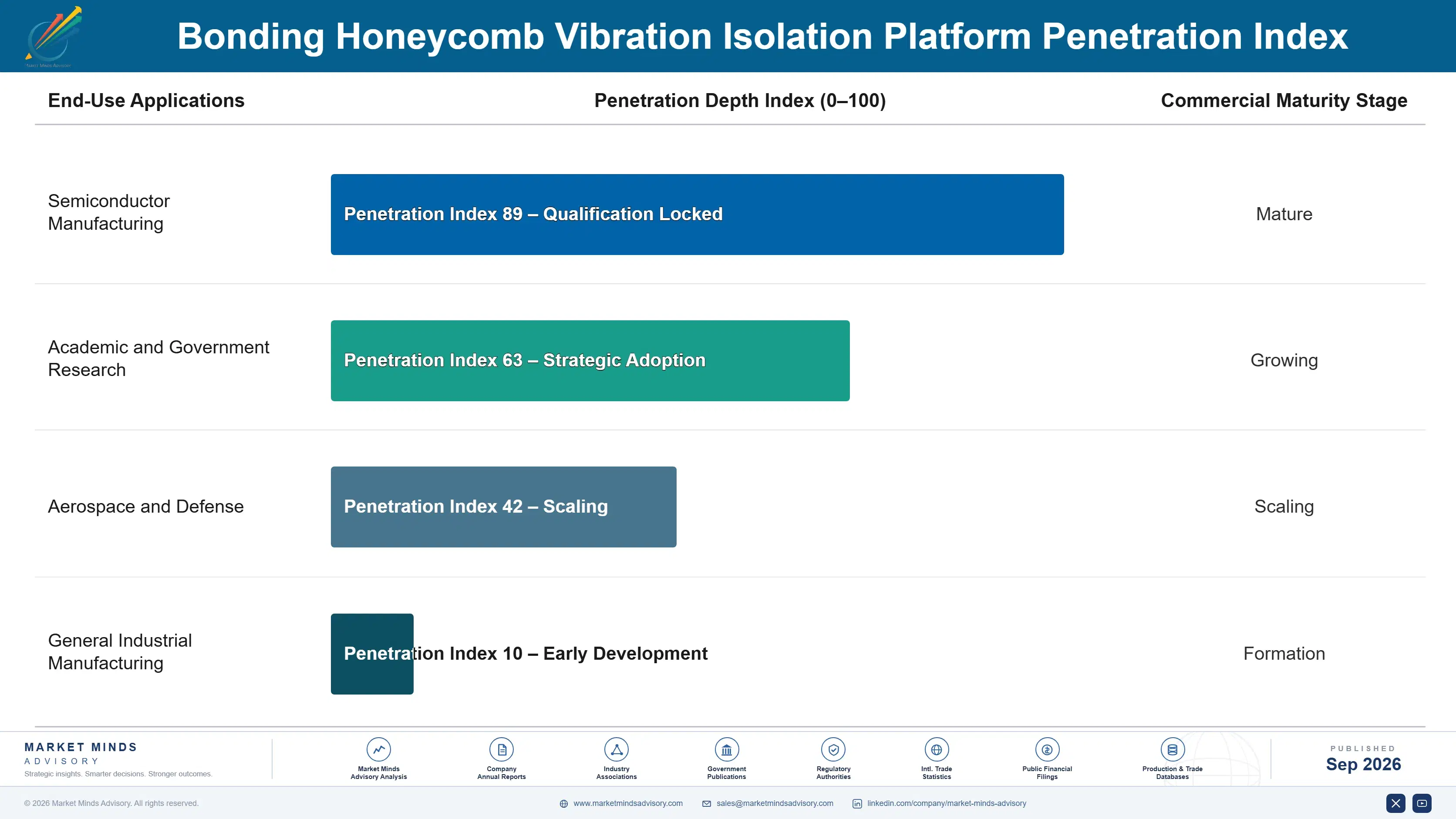
Semiconductor fabs are pushing lithography tool precision requirements into sub-nanometer territory as chip geometries continue shrinking, moving isolation platform specification well beyond the general industrial vibration damping that dominated the category for decades. This shift mirrors similar precision escalation seen in earlier lithography node transitions, where each generation of smaller chip geometries demanded correspondingly tighter mechanical stability from every piece of supporting fab equipment. Manufacturers investing early in ultra-precision bonding testing and long-term stability documentation are capturing disproportionate premium contract share, particularly in leading-edge fabs where micro-vibration failure directly threatens production yield and unit economics.
Market Impact: Adds 17 percent to fab demand