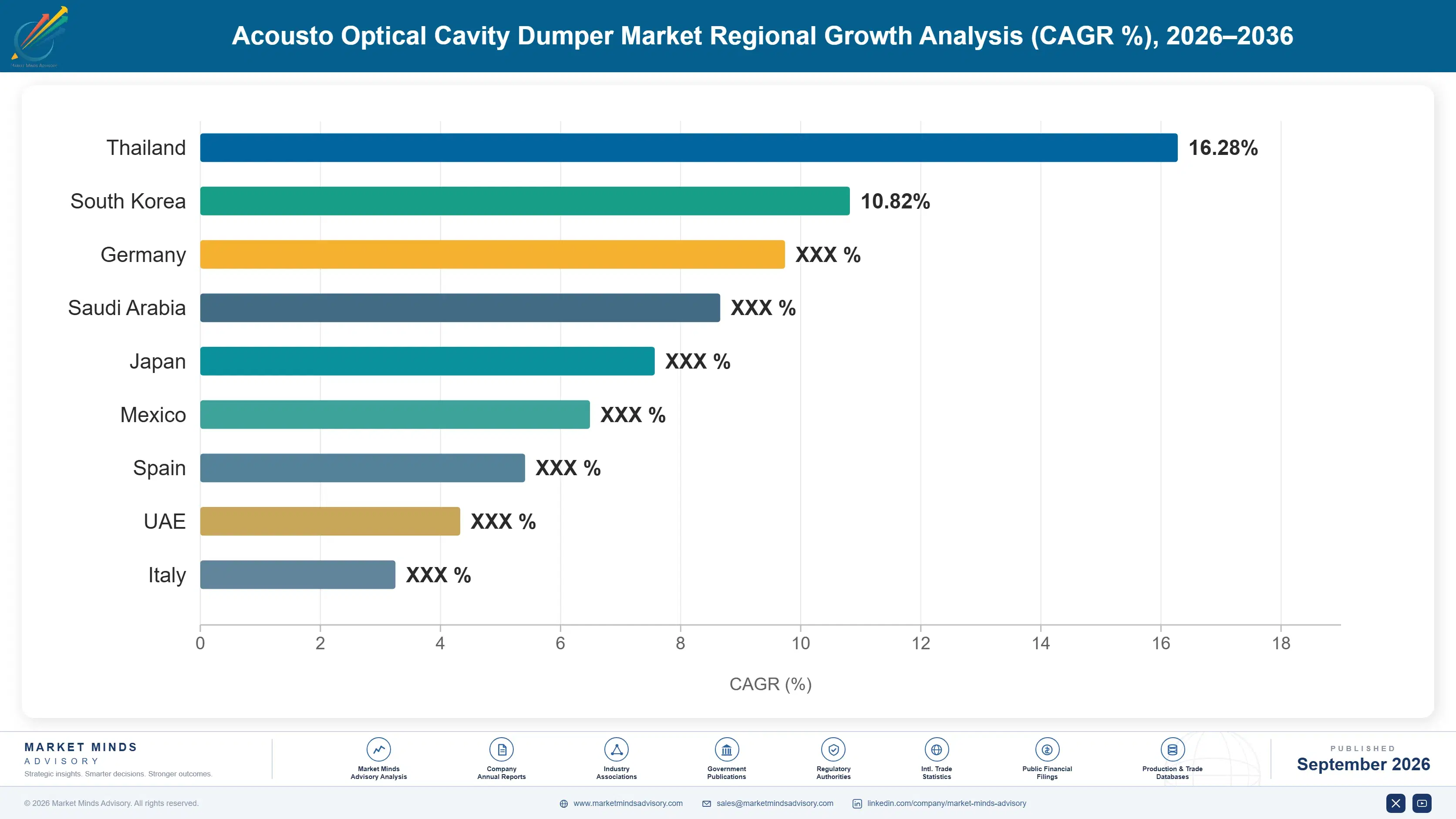
Semiconductor Metrology Tools Drive New Design Wins
Leading-edge chip fabrication facilities are installing advanced optical inspection and metrology tools at a rapidly increasing rate as node transitions demand tighter defect detection tolerances, and many of these tools rely on cavity-dumped laser sources for high-repetition-rate pulse generation. Taiwan Semiconductor Manufacturing Company and Samsung Foundry both expanded metrology tool orders meaningfully across 2025 as advanced packaging investment accelerated. This shift is pulling cavity dumper component demand into a customer segment that barely existed for this technology a decade ago, forcing suppliers to build semiconductor-industry sales relationships from scratch rather than relying on legacy distribution channels.
Market Impact: Industrial design wins grew 16 percent