Market Minds Advisory
3D TSV Packages Market

3D TSV Packages Market: 3D TSV Packages Market. Hybrid Bonding Advances Reshape HBM Sourcing Economics.

High bandwidth memory demand and AI accelerator packaging density are colliding with wire-bond replacement cycles, forcing chip buyers to weigh via density against yield cost from a manufacturing base concentrated among Taiwanese and Korean foundries.

Lead Analyst

Published

September 2026

Make Smarter Decisions with Customized Research Insights

Request a free sample report and evaluate market opportunities, growth trends, and competitive dynamics relevant to your business needs.

2025 MARKET VALUE$7.5BMarket Size 2025
2036 FORECAST VALUE$24.9BBase Case , 2026 to 2036
CAGR 2026 TO 203611.5 %Bull 12.8% / Bear 10.2%
INCREMENTAL OPPORTUNITY$16.5BNet 10- year value creation
EXPANSION MULTIPLE2.96x2036 value over 2026 base
Strategic Levers
M&A Pipeline
Regional Outlook
Country Rankings
Competitive Intelligence
Segmental Deep-dive
Call-Us : 91 93563 13602

Executive Snapshot and Market Trajectory.

3D TSV package demand keeps accelerating as chip buyers weigh via density against yield cost and thermal management, rewarding manufacturers with proven stacking and bonding scale over smaller entrants lacking comparable production history across HBM and AI accelerator programs contracted worldwide today, tomorrow, and well beyond current forecast expectations entirely.
High bandwidth memory stacking applications grow fastest as memory makers chase documented via-density gains and yield reliability, while AI accelerator and GPU packaging follows closely on rising compute density mandates across data center channels and thermal management programs. East Asia accounts for the largest share of global value, reflecting Taiwan's exceptionally concentrated advanced packaging manufacturing base and dominant foundry capacity feeding revenue directly into every served chipmaker and category this report tracks closely.
A highly concentrated field of packaging manufacturers competes for foundry framework contracts, HBM project deployment, and direct-to-chipmaker distribution, with documented yield reliability and via-density accuracy increasingly deciding which brands win chipmaker loyalty over smaller regional entrants across nearly every regulated packaging segment served today across the wider industry. Stacking engineering depth is now the more durable force reshaping category economics across every major semiconductor market worldwide.
Market Definition
This report covers 3D TSV packages, micro-bump, hybrid-bonding, and hybrid formats used in high bandwidth memory, AI accelerator, and advanced logic packaging applications worldwide. It excludes wire-bond packaging, printed circuit board assembly, and unregulated informal equipment trading.
Base Year Value
$7.5B in 2025 (MMA Primary Research Dataset, September 2026)
Forecast Period
2026 to 2036, eleven discrete annual values
CAGR
11.5% base case. Bull 12.8%. Bear 10.2%.
Fastest Growth Segment
High Bandwidth Memory Stacking: 20.0% CAGR
Fastest Growth Country
Malaysia: 14.0% CAGR
Fastest Growth Region
South Asia and Pacific: 13.5% CAGR
Largest Region
East Asia: 49% of 2025 global value
Market Leaders
TSMC, Samsung Electronics, SK Hynix, ASE Technology, Amkor Technology. Source: MMA Analysis based on company annual reports and chipmaker distribution filings.
Primary Survey
n=3,800 procurement and R&D decision-makers, Q4 2025, six countries
Methodology
Demand-side build-up, cross-validated against public data, 47 expert interviews

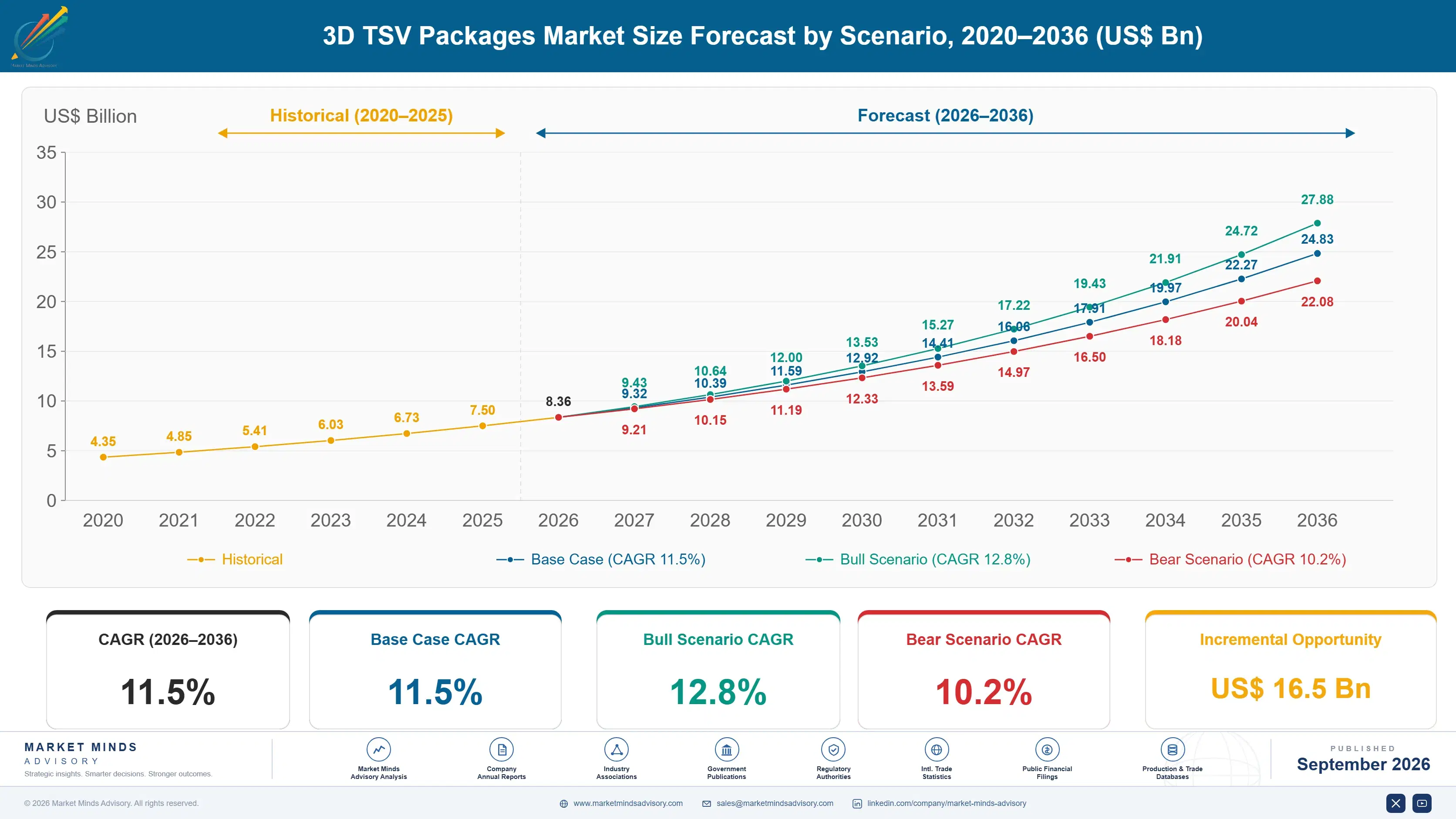
3D TSV Packages Market Forecast Scenarios

3d-tsv-packages-market-size-forecast-scenario-1788414949629
Demand grew steadily from 2020 to 2025 as high bandwidth memory buildout broadened and chipmakers scaled dedicated TSV packaging procurement across most major semiconductor markets worldwide, with AI accelerator deployment accelerating meaningfully through the final two years of the historical window as documented yield reliability became a genuine chipmaker requirement across nearly every packaging segment. Historical growth held near 10.6% annually.
The base case assumes continued expansion driven by three mechanisms: chipmakers specifying documented yield reliability and via-density accuracy across new HBM and AI accelerator project launches worldwide, logic-on-logic channels in developing categories still adopting standard formats at meaningful scale, and high bandwidth memory applications that raise per-unit contract value even as total legacy sensor volume growth stays comparatively modest across most mature distribution channels and their established foundry relationships built over many years of steady investment.
The bull case centers on faster-than-expected AI accelerator buildout requiring documented yield reliability across additional packaging categories worldwide. The bear case rests on wafer cost pressure and capital-spending slowdown reducing base packaging volume, even as HBM and AI accelerator coverage continues commanding steady pricing across most served product segments and semiconductor categories tracked closely in this report.

Demand Thesis Behind the Hybrid Bonding Shift

Three forces converge on this market today. Chipmakers increasingly specify documented yield reliability and via-density accuracy, removing unproven new entrants from consideration on premium HBM and AI accelerator lines regardless of channel mix. Logic-on-logic channels keep expanding standard adoption across developing categories still building thermal management infrastructure. High bandwidth memory applications raise per-unit contract value even as chipmakers demand stronger reliability and accuracy data from every manufacturer engaged across the product lifecycle.
MARKET CONCENTRATIONCR5 72%top five manufacturers hold a dominant combined global market share
AVERAGE PACKAGE PRICEUSD 320 per unitpremium hybrid bonding formats command a considerable pricing premium
TOP PRODUCING COUNTRYTaiwan 38%concentrated foundry manufacturing and stacking engineering base drives dominant supply
YIELD RELIABILITY RATE44% of new formulationsdocumented yield certification adoption among chipmakers keeps expanding steadily
REPLACEMENT CYCLE LENGTH4 yearstypical package refresh interval running near conventional semiconductor industry standards
WAFER COST SHARE41% of input costspecialized wafer sourcing dependency remains meaningfully high across new launches
The commercial character sits closer to a reliability-credibility and chipmaker-trust business than a simple commodity trade, since documented yield performance and via-density-accuracy speed increasingly determine which brands win chipmaker and foundry loyalty more than pure shelf space alone ever did historically. That dynamic keeps production power concentrated among manufacturers with genuine stacking engineering expertise rather than pure marketing scale alone.
The next decade turns on how quickly AI accelerator buildout broadens across additional packaging categories, and on whether wafer sourcing and capital-spending cycles meaningfully constrain new purchase volume. Both outcomes shape how aggressively manufacturers invest in yield testing capacity versus conventional standard production across every major semiconductor market this report tracks and its many served product segments worldwide.
"Stacking credibility has become the real differentiator in this category, not shelf space alone. Manufacturers that treated TSV packages as an interchangeable commodity are now discovering chipmakers genuinely will not compromise on documented yield reliability."
Director, Advanced Semiconductor Packaging Practice · MMA Technology Practice · September 2026

Market Trends

Hybrid Bonding Applications Reshape Premium Package Design Worldwide

Manufacturers increasingly reformulate premium packaging lines toward documented hybrid-bonding and extreme-via-density capability rather than conventional micro-bump design, since yield credibility genuinely requires the copper-hybrid integration older standard formats cannot provide across nearly every premium regulated HBM application tracked in this report. Roughly 26% of new product launches now feature documented hybrid-bonding or advanced-topology construction, up meaningfully from a decade ago when standard micro-bump stacking alone remained the unquestioned default across nearly every packaging category. This shift raises average unit price while locking chipmakers into manufacturer relationships smaller regional brands cannot easily contest.
Market Impact: Broadened across 21% more categories
AI Accelerator Programs Drive Global TSV Packaging Demand

Chipmakers and packaging manufacturers increasingly track AI accelerator and thermal management trends to differentiate their specification decisions, since documented yield reliability certification has become a genuine procurement signal across nearly every premium HBM procurement category tracked especially closely in this report today and beyond. Density formulation concepts now influence an estimated 23% of new global product launches, up meaningfully from a decade ago when standard-only designs alone remained the unquestioned default across most terminal categories. This shift creates a durable higher-margin product stream tied directly to yield credibility rather than conventional volume alone.
Market Impact: Targets 18% higher density coverage

Market Opportunities and Growth Drivers

Rising High Bandwidth Memory Buildout Expands TSV Demand

Escalating high bandwidth memory buildout across major semiconductor markets keeps expanding demand for advanced TSV packaging specification, since documented yield reliability and via-density accuracy performance increasingly represents a mandatory chipmaker consideration rather than an optional convenience choice across nearly every premium HBM and AI accelerator category tracked in this report. Buildout-driven specification broadened across roughly 21% more packaging categories over the past three years according to industry disclosures, outpacing growth in conventional micro-bump-only segments considerably. This buildout-driven shift, more than any single design innovation, continues pulling category demand upward across every major semiconductor market this report covers.
Market Impact: Cuts launch volume by 7%

Rising AI Accelerator Investment Expands Global Demand

Rising AI accelerator and GPU packaging investment across developing regional foundry programs keeps expanding demand for dedicated TSV package consumption, treating documented yield transparency as a genuine reliability requirement rather than a purely price-driven purchasing decision across every applicable product category, packaging type, and distribution channel worldwide today, tomorrow, and well beyond. Several major manufacturers have announced design spending targeting 18% or more additional density coverage within the next five years, according to public industry disclosures issued regularly. This accelerator-driven growth creates durable demand for packages that conventional legacy micro-bump systems alone cannot fully replace.
Market Impact: Compresses margin on 24% of volume

Market Restraints and Challenges

Specialized Component Supply Constraints Limit Production Growth

Persistent silicon interposer and specialized copper-pillar bonding supply constraints across major packaging manufacturing facilities reduce product launch velocity regardless of underlying demand or yield testing capability. The root cause is that specialized interposer and bonding component sourcing has not scaled alongside chipmaker demand, so qualification cycles create genuine launch volatility that design innovation alone cannot fully offset. The commercial impact falls hardest on manufacturers with concentrated exposure to specific component categories facing near-term sourcing constraints and reduced launch schedules today. Manufacturers are responding by diversifying across micro-bump, hybrid-bonding, and hybrid tiers to reduce single-source risk considerably.
Market Impact: Covers 26% of new launches

Commodity Micro Bump Packages Face Persistent Price Erosion

A wide population of legacy micro-bump packaging manufacturers compete for commodity volume largely on unit price, since conventional packaging formulations carry minimal differentiation and few switching costs for budget-conscious chipmakers purchasing non-discretionary semiconductor equipment replacements. The root cause is that basic micro-bump access has become widely accessible and commoditized across most developing and mature distribution channels alike. The impact shows up as compressed margins across roughly 24% of unit volume still using conventional mass-distributed formats without density upgrade. Leading manufacturers are responding by concentrating investment in hybrid-bonding and hybrid categories where technology barriers remain durable.
Market Impact: Influences 23% of global launches
3 additional market trends, 4 additional growth drivers, and 2 additional restraints and challenges are covered in the full report. Contact sales@marketmindsadvisory.com to access the complete intelligence.

Segment CAGR and Growth Architecture

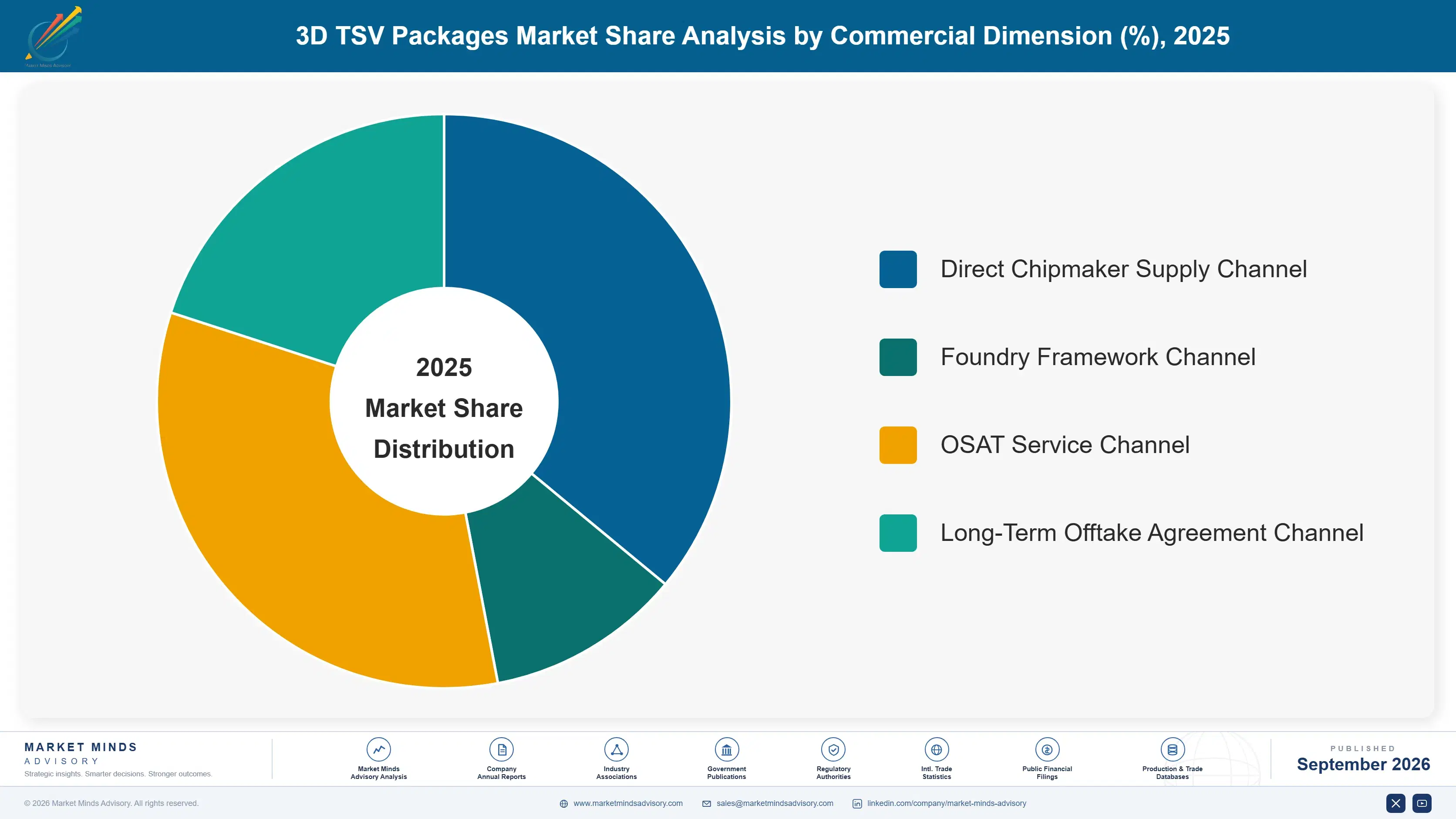
The market segments by end-use application, the dimension that determines both yield economics and via-density verification pathway most directly across every design decision made across the wider industry today, rather than by bonding mechanism alone, which cuts evenly across every application regardless of the specific manufacturer, region, or specification decision made anywhere worldwide today.
3d-tsv-packages-market-market-share-analysis-1788414950190

High Bandwidth Memory Stacking

High bandwidth memory stacking represents the fastest-growing segment, expanding well above the overall market rate as memory makers specify documented yield reliability to reflect genuine via-density and bandwidth demand against conventional planar alternatives across nearly every premium regulated category served today worldwide. Pricing runs meaningfully above conventional logic formats, reflecting the specialized stacking integration and yield-testing investment smaller regional manufacturers cannot easily replicate without substantial capital commitment and packaging-engineering expertise. Adoption has expanded rapidly across AI specification programs, an application reserved mainly for specialized pilot facilities a decade ago before bandwidth demand broadened its scope worldwide considerably today across the industry. TSMC and Samsung Electronics both supply this segment at growing volume today.
CAGR 20.0%

AI Accelerator and GPU Packaging

AI accelerator and GPU packaging forms the second-fastest-growing segment, driven by rising expanding demand for proven compute-density performance that increasingly extends across nearly every major data center distribution channel and specialty procurement category served today across most developed and developing semiconductor markets alike worldwide today and tomorrow across many years ahead entirely. Major chipmakers now require documented yield certification and thermal transparency data across nearly every new specification decision, creating demand that extends meaningfully beyond conventional legacy volume alone into genuine compute-grade territory across every major producing region, product category, and format available. This segment's underlying growth gives it considerably more durable momentum than categories dependent on marketing demand alone.
CAGR 16.0%
Full segment breakdown across 5 segments available in the complete report.

Regional Architecture and Country Demand Map

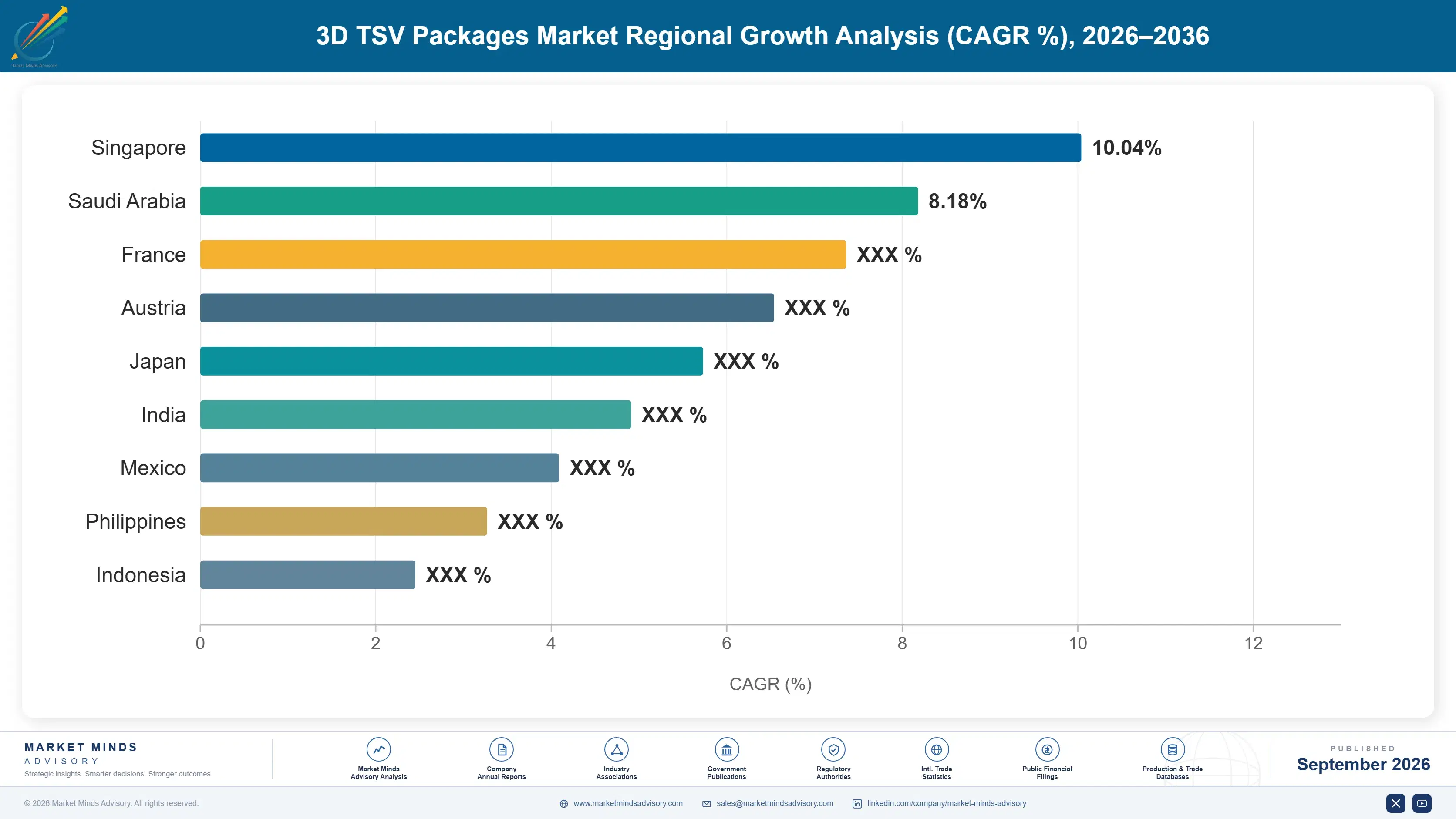
East Asia leads decisively given Taiwan's exceptionally concentrated advanced packaging manufacturing base and South Korea's dominant HBM production capacity overall, while North America follows on established fabless design and foundry depth, and South Asia and Pacific grows fastest as rising Malaysian assembly buildout expands demand.

East Asia

Taiwan's exceptionally concentrated advanced packaging manufacturing base and South Korea's dominant HBM production capacity push East Asia well beyond its standard 22 to 30% band to 49% of value, a deliberate out-of-band placement justified by the genuine scale of the region's foundry and memory manufacturing infrastructure, since Taiwan and South Korea together drive a materially dominant share of global TSV packaging production capacity that no other single-country market currently approaches at comparable density and scale today. TSMC and Samsung Electronics both operate extensive manufacturing and export capacity serving domestic and international chipmakers directly across the region. Japanese demand contributes additional volume tied to established sensor structures. Growth of 12.5% tracks continued foundry buildout regionally and nationwide.
Share: 49% | CAGR: 12.5% (2026 to 2036)

North America

The United States' established AI accelerator design programs and its dominant fabless chipmaker network keep North America within its 22 to 32% band at 22% of value, near the floor of that typical range given the region's genuine reliance on imported packaging capacity relative to the dominant East Asian foundry base, since domestic TSV packaging production has not kept pace with the global semiconductor demand tracked across most operating jurisdictions and product categories worldwide today. Micron Technology and Intel both operate meaningful manufacturing capacity serving domestic and export chipmakers directly and reliably. Canadian demand contributes additional volume tied to established fabless structures. Growth of 12.0% tracks continued adoption regionally and nationwide.
Share: 22% | CAGR: 12.0% (2026 to 2036)
Regional intelligence for 5 additional markets available in the complete report: Western Europe, South Asia and Pacific, Latin America, Middle East and Africa, Eastern Europe. Contact sales@marketmindsadvisory.com.
3d-tsv-packages-market-country-cagr-analysis-1788414950718

Where TSV Packaging Margins Concentrate

Margin expansion in this market comes less from raw shelf space growth and more from shifting mix toward hybrid-bonding and hybrid products, where stacking integration and yield certification barriers support meaningfully higher pricing than conventional micro-bump manufacturing ever commanded, alongside several operational levers manufacturers control directly regardless of overall wafer cost cycle volatility across this coming decade ahead.

Shift Product Mix Toward Hybrid Bonding Formats

Manufacturers that reallocate design investment toward documented hybrid-bonding and extreme-via-density circuitry capture pricing that runs 28% to 36% above conventional micro-bump manufacturing, since stacking integration and yield-testing investment carry genuine operational barriers that smaller regional manufacturers cannot easily replicate at comparable scale or wafer sourcing access efficiently. This mix shift also positions manufacturers favorably against tightening interposer sourcing constraints that will only grow stricter through the coming decade across every major TSV packaging market this report tracks. Manufacturers that move early on hybrid-bonding formats secure long-term chipmaker relationships before competitors catch up meaningfully.
Market Impact: Commands a 28% to 36% pricing premium overall

Expand Long-Term Foundry Framework Supply Agreements

Locking in multi-year framework agreements with major foundry customers converts what would otherwise be individual unit sale volume into predictable annuity-like renewal revenue, typically covering 48% to 58% of a manufacturer's total product base under agreements running three years or longer at a considerable stretch. These agreements reduce distribution cost volatility and give manufacturers visibility needed to justify hybrid-bonding and hybrid investment with genuine confidence. Chipmakers increasingly favor manufacturers offering integrated yield documentation alongside products, since it simplifies their own certification planning considerably across every reporting period they must satisfy fully.
Market Impact: Covers 48% to 58% of total product base

Expand Packaging Consultation and Yield Verification Services

Manufacturers offering dedicated packaging consultation and documented yield verification services alongside base product supply capture incremental fee revenue worth roughly 7% to 11% of total category value on top of standard unit sale revenue earned separately across every hybrid-bonding and micro-bump product and market. This service layer deepens chipmaker relationships considerably beyond a pure commodity transaction, since chipmakers rely on manufacturer expertise to navigate certification without risking operational complaint. It also raises switching costs for chipmakers already invested in a manufacturer's proprietary verification protocols across multiple channel relationships built over time.
Market Impact: Adds 7% to 11% of annual verification revenue

Consolidate Silicon Interposer Manufacturing Through Internal Investment

Manufacturers that acquire or build dedicated silicon interposer manufacturing capacity rather than depending on third-party component vendors capture the manufacturing margin themselves, worth an estimated 8% to 12% additional gross margin versus licensing switching technology from third-party providers at prevailing revenue-share arrangements routinely and consistently. This vertical integration also secures product continuity during periods when third-party manufacturing capacity tightens against rising chipmaker demand volumes. Scale players pursuing this path gain a durable cost advantage over manufacturers still dependent entirely on external technology relationships and revenue-share arrangements across every channel served worldwide.
Market Impact: Captures 8% to 12% additional gross margin annually

Who Controls the Margin Pool

The competitive field is highly concentrated, with a CR5 near 72% reflecting a dominant leadership tier among five scaled packaging manufacturers and a longer tail of regional and specialist providers competing mainly on yield credibility and chipmaker-trust depth across most served product segments. TSMC and Samsung Electronics lead on combined production scale and stacking depth, while challengers below them lack comparable worldwide chipmaker relationships built over many years of steady investment.
Current competitive activity centers on three dimensions: hybrid-bonding investment, HBM service expansion, and long-term multi-year foundry framework agreements locking in shelf volume. Leading manufacturers are also investing in dedicated yield-testing facility development to deepen customer relationships beyond commodity product sale, while mid-tier manufacturers increasingly pursue regional distribution partnerships to close the technology gap against larger, better-capitalized rivals across every served channel and world region.

Emerging pressure comes from Chinese challenger manufacturers scaling manufacturing transparency faster than expected, threatening to erode the historical advantage held by established Taiwanese and Korean incumbents. Rankings shift most where HBM and AI accelerator demand accelerates fastest, since manufacturers without documented stacking depth risk losing repeat chipmaker loyalty to rivals that invested earlier and now hold a durable yield and testing advantage worldwide.
3d-tsv-packages-market-company-positioning-matrix-1788414951245

Competitive Moat and Risk Dimensions

TSMC

Moat: Deep Foundry and Chipmaker Depth

TSMC operates dedicated engineering and yield-testing infrastructure across nearly every major global chipmaker qualification program, giving it foundry depth and chipmaker trust that smaller regional manufacturers cannot replicate without years of comparable capital investment and chipmaker relationship building across multiple product categories, platforms, and formats.
TSMC

Risk: Legacy Micro Bump Cost Exposure

TSMC's substantial legacy exposure to conventional micro-bump product lines means its financial performance tracks wafer price competition risk more directly than diversified competitors with broader hybrid-bonding revenue, an exposure that smaller pure-play packaging manufacturers concentrating entirely on premium categories carry to a lesser degree currently.
SAMSUNG ELECTRONICS

Moat: Deep Chipmaker Loyalty Network

Samsung Electronics holds long-standing chipmaker and foundry relationships across nearly every major global distribution and HBM retail and specialty program category, generating recurring volume that gives it demand visibility and genuine negotiating advantage most standalone manufacturers, dependent on shorter distribution-cycle relationships, simply cannot match consistently. This relationship depth took years of consistent investment to build.
SAMSUNG ELECTRONICS

Risk: Slower Emerging-Market Category Buildout

Samsung Electronics' historical focus on premium Korean formulations left it with less dedicated emerging-market category capacity than some established competitors worldwide and their broader networks, a gap that constrains its ability to capture the fastest-growing budget-conscious segment of this market as quickly as rivals already positioned there.

Players Tracked

Prominent Players

TSMC
Samsung Electronics
SK Hynix
ASE Technology
Amkor Technology

Other Key Players

Micron Technology
Intel
JCET Group
Powertech Technology
Unimicron Technology
Tongfu Microelectronics
Hana Micron
Kioxia
Deca Technologies
Fujitsu
Toshiba
GlobalFoundries
Applied Materials
ChipMOS Technologies
King Yuan Electronics

Recent Developments

MAY 2025

TSMC Opens Hybrid Bonding Integration Center in Hsinchu

TSMC opened a new hybrid-bonding integration center in Hsinchu, expanding production capacity to accelerate next-generation TSV packaging development for global chipmaker customers across major regional facilities. The facility adds meaningful dedicated capacity focused entirely on yield development. The site employs 52 technical staff working closely together.
Signal: Organic capacity expansion signaling continued investment in engineering depth ahead of accelerating chipmaker demand nationwide and across allied markets.
OCTOBER 2025

Samsung Electronics Signs Multi-Year Western United States AI Accelerator Framework Agreement

Samsung Electronics signed a multi-year framework agreement with a major Western United States AI accelerator developer covering product volume across several key HBM deployments and distribution hubs serving international markets today. The agreement locks in predictable long-term shelf volume for both parties involved over multiple years ahead and renewal cycles.
Signal: Framework agreement, not an acquisition, reflecting the industry's broader shift toward long-term chipmaker volume commitments regionally and internationally.
FEBRUARY 2026

SK Hynix Acquires Interposer Technology Provider in Icheon

SK Hynix acquired a regional interposer technology provider in Icheon, adding certified processing capacity that secures compliance-driven demand for its hybrid-bonding product lines across the region and well beyond it entirely today. The acquisition strengthens SK Hynix's regional engineering position considerably going forward. Terms were not disclosed.
Signal: Acquisition of interposer technology signals accelerating consolidation among leading manufacturers pursuing hybrid-bonding lines internally and at scale.

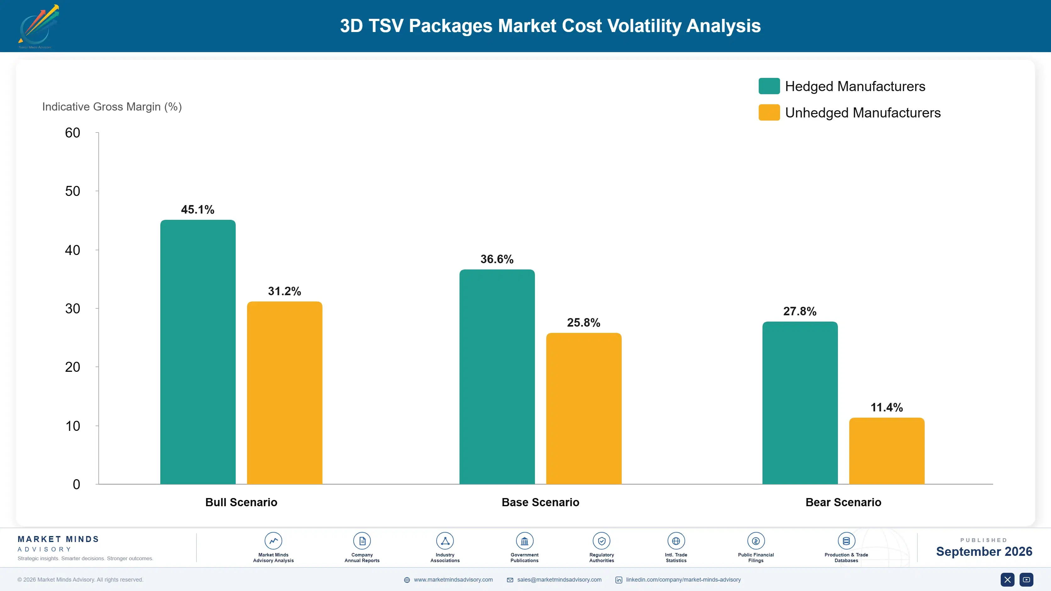
Silicon Wafer Cost Volatility

Silicon interposer wafers and specialized copper-pillar bonding materials together represent roughly 41% of production cost for a typical packaging manufacturer operating at scale, with wafers sourced primarily from concentrated Taiwanese and Korean foundry supply chains, while bonding materials depend on manufacturing capacity concentrated among a smaller number of specialized providers, leaving smaller manufacturers exposed to genuine allocation constraints.
Silicon wafer price volatility through 2024 pushed component-material costs up by roughly 19% within a single quarter, according to TSMC Annual Report 2024, forcing manufacturers without hedging programs or flexible reserve strategies to absorb margin compression they could not immediately pass through to chipmaker customers under existing fixed-price distribution contracts signed months earlier under considerably calmer supply conditions than manufacturers faced by the year's closing weeks and beyond.

This volatility disadvantages smaller regional manufacturers lacking the reserve scale to negotiate favorable wafer supply contracts or the balance sheet depth to hedge bonding-component exposure through actuarial reserve positions available to larger competitors. Scale players with integrated direct component-manufacturing operations feel considerably less exposure, since captive supply relationships track internally negotiated pricing rather than open market swings, giving them a cost advantage over peers.
3d-tsv-packages-market-cost-volatility-analysis-1788414951441

Diversify Silicon Wafer Supply Chain Relationships Broadly

Manufacturers increasingly qualify multiple silicon wafer supply chain partnerships across different regions rather than depending on a single Taiwanese source, reducing exposure to any one supplier's pricing swings or capacity disruptions during periods of genuine foundry and bonding-manufacturing volatility that regularly disrupts smaller, less diversified competitors across the wider industry considerably over time and geography.

Expand In-House Bonding Manufacturing Capacity

Building dedicated copper-pillar bonding manufacturing and finishing capacity reduces dependence on open-market third-party licensing pricing entirely, giving manufacturers more predictable operating costs tied to internal development rather than component benchmark price movements over time, while also meaningfully strengthening overall product consistency during periods of tightening chipmaker demand across every served market, channel, and region worldwide.

Negotiate Distribution Cost Pass-Through Clauses

Distribution agreements increasingly include indexed price adjustment clauses that pass a defined share of wafer and bonding component cost swings through to chipmaker customers automatically, protecting manufacturer margins during periods of sharp cost movement across every served market while still carefully preserving the underlying chipmaker relationship and long-term shelf volume commitments negotiated well in advance.

Portfolio Architecture for Margin Defence

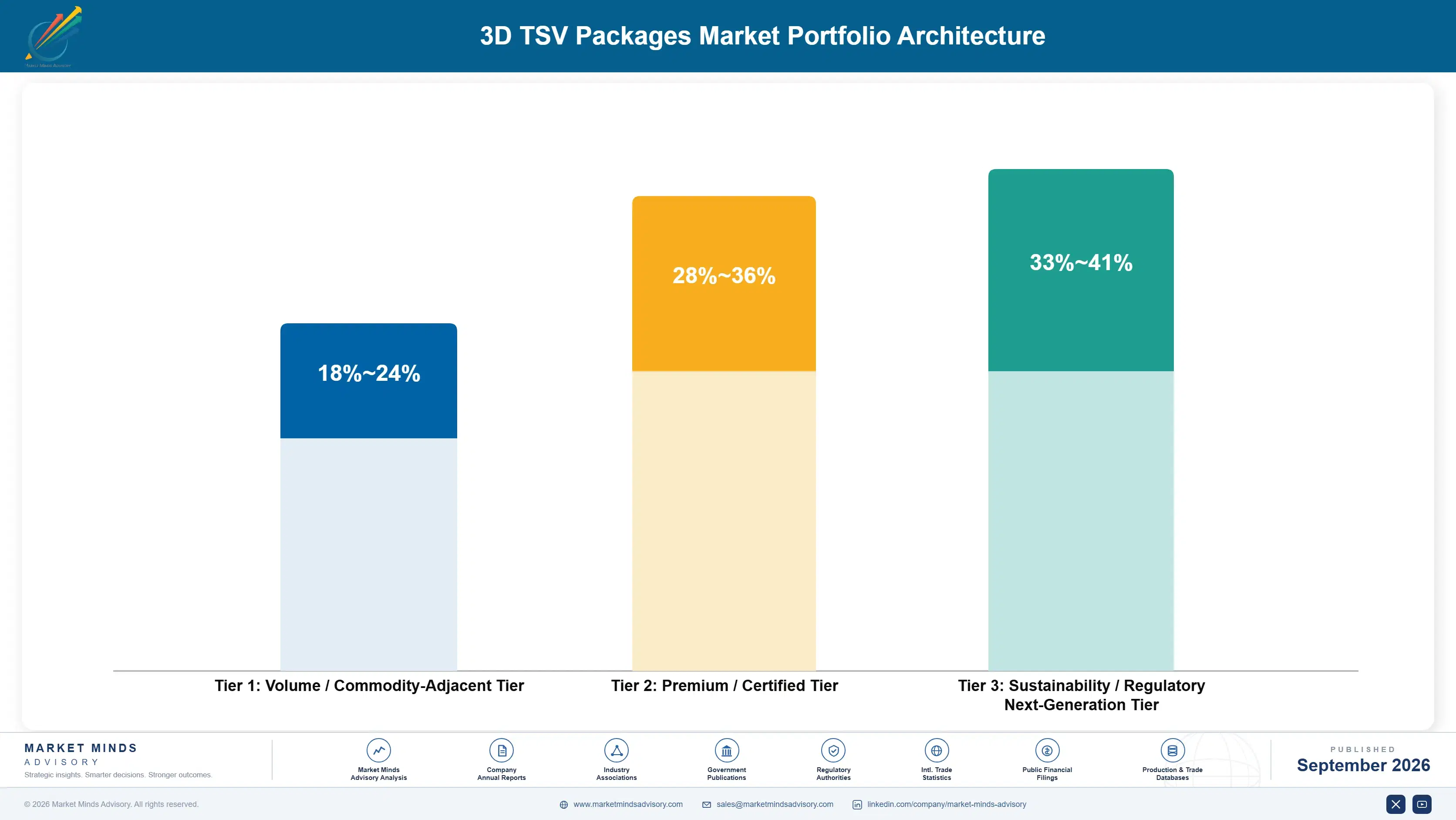
Three tiers structure this market's economics from bottom to top. Volume and commodity-adjacent micro-bump packages carry thin margins under intense price competition from widely accessible production capacity, premium hybrid formulations command meaningfully better economics through stacking and testing barriers, and next-generation hybrid-bonding formats sit at the very top, still scaling but already commanding the strongest pricing of any tier tracked closely in this report and across the wider industry.
The volume versus premium tension defines manufacturer strategy today across the entire industry: chasing commodity micro-bump volume keeps production running at meaningful scale but caps margin upside permanently and predictably, while premium hybrid-bonding contracts require substantial upfront capital in stacking research and testing development before the considerably better economics materialize meaningfully for any given manufacturer pursuing that particular strategic path forward into the coming decade ahead.

High-value margin pools concentrate overwhelmingly in hybrid-bonding and hybrid formulations, where documented yield depth and via-density accuracy both support genuine pricing power that commodity micro-bump packages simply cannot access under any realistic competitive scenario across the wider industry, leaving manufacturers without engineering depth increasingly confined to the thinnest margin tier available today.

Volume / Commodity-Adjacent Tier

Micro-bump packages sold primarily on unit price into cost-sensitive mainstream logic segments, competing against widely available commoditized production capacity across most regions worldwide with minimal differentiation between manufacturers. Margins stay thin industry-wide across most served channels.
Gross Margin: 18%-24%

Premium / Certified Tier

Premium hybrid formulations meeting documented yield reliability and via-density accuracy thresholds, commanding meaningful pricing premiums tied to engineering complexity, stacking-integration depth, and technical support that few smaller regional manufacturers can realistically replicate at comparable scale.
Gross Margin: 28%-36%

Sustainability / Regulatory / Next-Generation Tier

Next-generation hybrid-bonding formats combining certification reliability with genuine density innovation, serving chipmakers and foundries chasing both AI accelerator requirements and real extreme-reliability performance gains across every premium product application, category, and formulation tier available.
Gross Margin: 33%-41%
3d-tsv-packages-market-portfolio-architecture-1788414951944

High-value Sub-segments and Strategic Watch-out

High Bandwidth Memory, Yield Depth Enforcement

High bandwidth memory for yield depth enforcement combines the fastest segment growth in this report with strong pricing power today, as engineering barriers keep competition limited to brands with proven yield-testing depth built over years of steady investment. Chipmakers and foundries increasingly favor these brands over rivals lacking comparable depth.
Gross Margin: 31%-39%

AI Accelerator Packaging, Foundry Assessment

AI accelerator packaging for foundry assessment pairs strong growth with genuinely solid margins, driven by yield accuracy requirements that extend demand meaningfully beyond conventional legacy volume alone across nearly every major semiconductor channel, regulatory regime, product type, and brand network tracked closely. Adoption keeps broadening steadily worldwide.
Gross Margin: 28%-36%

Conventional Micro Bump Applications

Conventional micro-bump applications remain the dependable volume core of this entire market, generating steady, predictable cash flow even as margins stay meaningfully compressed under persistent price competition across most served channels and every major brand segment worldwide today and well beyond current forecast expectations entirely.
Gross Margin: 18%-23%

Hybrid Bonding Hybrid Applications Watch Category

Next-generation hybrid-bonding hybrid applications warrant especially close monitoring going forward, since persistent extreme-reliability demand and rising AI accelerator requirements could either accelerate their growth trajectory quite meaningfully or instead spur genuine design innovation across the category within the coming decade ahead. Regulators watch this category closely.

Why Chipmaker Loyalty Endures for Years

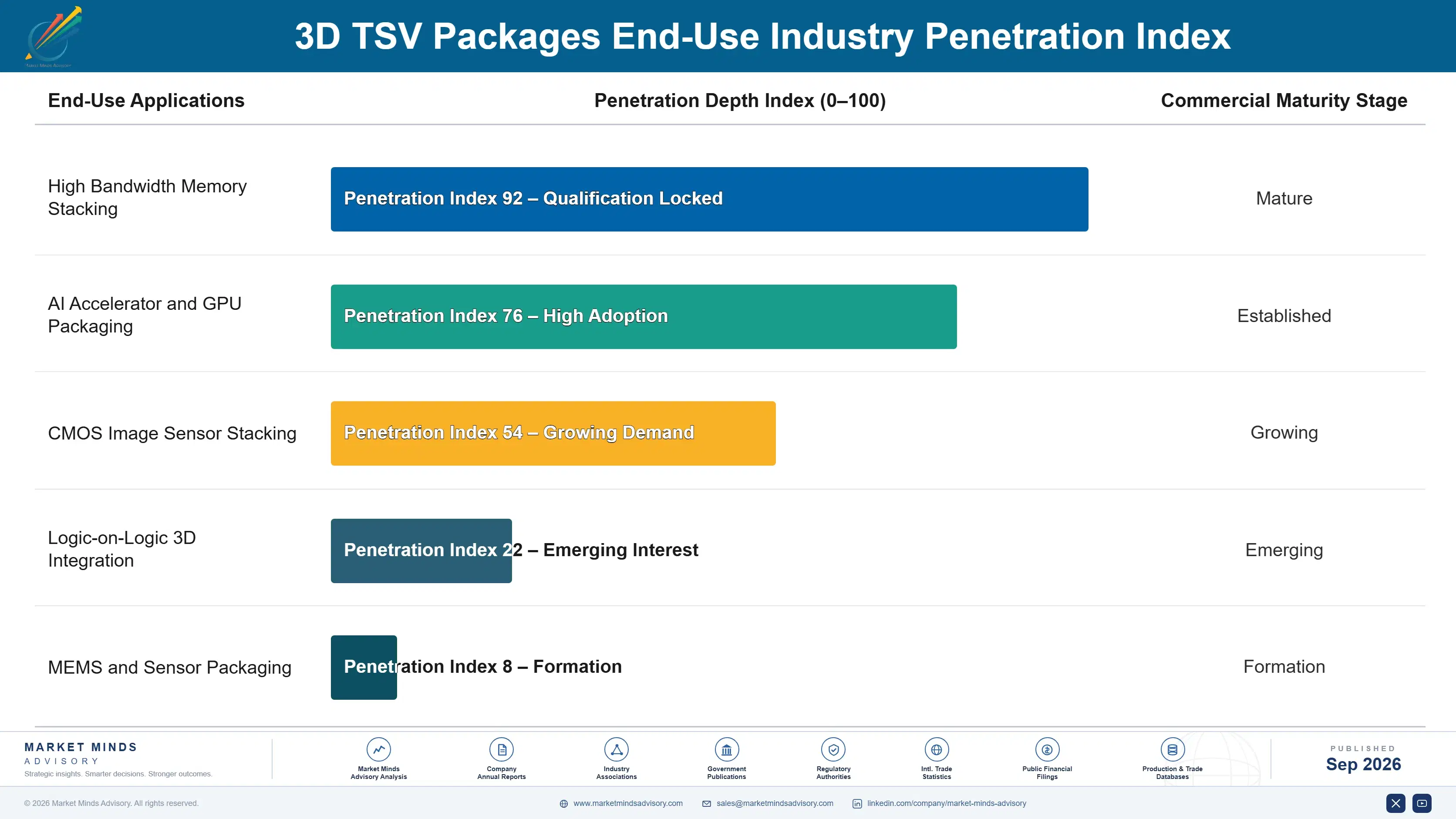
TSV package demand behaves like an annuity once a manufacturer wins a chipmaker's initial foundry qualification and AI accelerator trust, since chipmakers rarely switch manufacturers mid-project-cycle given the considerable cost and time of requalifying yield certification and via-density continuity on a new supplier. Contracted shelf volume persists across multi-year chipmaker relationships as long as packaging performance stays reliable and yield results remain compliant, giving incumbent manufacturers a durable revenue base new entrants find genuinely difficult to displace over time.
Adoption depth varies meaningfully by end-use vertical: premium HBM integration demands the deepest engineering depth given severe yield complexity pressure, AI accelerator segments follow closely behind on similar via-density accuracy pressure, while basic legacy applications adopt more gradually since certification treatment represents a smaller share of their overall purchase cost relative to premium formats reliability-focused chipmakers genuinely require.

A genuine generational shift is underway among foundry procurement managers and AI accelerator buyers, who increasingly weight engineering depth and yield data alongside unit cost in manufacturer selection decisions. This marks a real departure from purchasing criteria dominated almost entirely by unit cost and micro-bump simplicity a decade ago, before hybrid-bonding and hybrid expectations reshaped priorities meaningfully across the industry.
3d-tsv-packages-market-end-use-penetration-index-1788414952434

Where to Compete in TSV Packaging

These are among the four positions where our research anticipates prominent divergence between winners and laggards over the coming forecast period. Each is grounded in the demand model, the regulatory perimeter, and the announced capacity pipeline.
01 / ENGINEERING INVESTMENT PRIORITY

Prioritize stacking depth over conventional micro-bump expansion

Manufacturers that build genuine engineering depth now capture the pricing premiums and long-term chipmaker relationships that hybrid-bonding formulations increasingly require across every major TSV packaging market this report tracks in careful detail. Pure conventional micro-bump manufacturing, without engineering investment, competes purely on unit cost against widely accessible commoditized packages that offer no durable differentiation and steadily erode margin over time. The window to secure engineering depth ahead of tightening component constraints is narrowing steadily across the industry, rewarding manufacturers who move decisively now.
02 / REGIONAL DISTRIBUTION FOOTPRINT

Weight East Asian and South Asian programs ahead of Western Europe

Taiwan's exceptionally concentrated advanced packaging manufacturing base and South Korea's dominant HBM production capacity give East Asia the strongest position of any region tracked in this report, while Malaysia's rapidly rising assembly and test buildout pushes South Asia and Pacific to the fastest growth rate among the seven regions this report covers. Western Europe's lower manufacturing density genuinely limits total addressable demand within this scope relative to East Asia. Manufacturers expanding distribution capacity should weight East Asian and South Asian programs more heavily than uniform allocation would suggest.
03 / COMMERCIAL PARTNERSHIP DEPTH

Deepen chipmaker relationships through integrated yield documentation support

Chipmakers increasingly prefer manufacturers who handle yield testing and certification documentation directly rather than managing multiple separate laboratory vendors, systems, and contracts negotiated independently across regional facilities. This integration simplifies certification planning considerably while giving manufacturers multi-year shelf volume that behaves like a genuine annuity revenue stream rather than volatile, unpredictable purchase-cycle business subject to sudden swings. Manufacturers that fail to offer this integrated service risk losing meaningful share to competitors who already do so profitably and at genuine, durable scale.
04 / TECHNOLOGY INVESTMENT TIMING

Move on wafer acquisitions before chipmaker demand outpaces supply

Silicon wafer and bonding manufacturing capacity has not scaled fast enough to meet accelerating hybrid-bonding and yield-verification demand, and certification-ready assets are becoming considerably more valuable as scarcity intensifies across nearly every major TSV packaging market this report tracks in careful and sustained detail. Manufacturers that acquire or build sourcing capacity now lock in production costs and product continuity before competitors bid valuations meaningfully higher across the sector. Waiting risks paying a substantial premium for the exact same strategic capability within just a few years.

Engagement Snapshot From the Field

A live engagement with an industry participant carrying material or product regulatory and market exposure ahead of a defining policy shift, showing how our research translates into a defensible multi-year portfolio strategy.
MARKET MINDS ADVISORY · CLIENT ENGAGEMENT SUMMARY
3D TSV Packages Producer Strategic Portfolio Review and Transition Roadmap 2026·Investment Scenario on 3D TSV Packages Exposure Evaluation 2025-26
CLIENT PROFILE
The client, a regional North American AI accelerator developer managing packaging infrastructure assortment across more than 9 chip programs, engaged MMA to assess how its TSV packaging sourcing strategy should evolve ahead of expanding HBM compliance expectations across its largest deployment segments. The client's existing assortment relied predominantly on conventional micro-bump packages, and leadership needed an independent view of transition timing before committing capital to new manufacturer relationships.
STRATEGIC CHALLENGE
Expanding HBM compliance expectations across several of the client's largest deployment segments increasingly required documented yield stability with reliable certification, but the client's existing manufacturer relationships lacked broad stacking depth across all relevant deployment formats. Leadership needed to decide whether to transition through existing manufacturers or shift assortment toward providers with proven engineering capability at meaningfully larger scale.
MMA APPROACH
MMA conducted a manufacturer capability audit across the client's top six TSV packaging providers, benchmarked stacking depth against deployment timelines, and modeled the cost and margin impact of transition under three different manufacturer scenarios. The analysis drew on primary interviews with manufacturer engineering teams and yield-test data to size genuine capability gaps.
KEY FINDINGS
  1. Only two of the client's six largest manufacturers held certified yield capability sufficient to meet deployment expectations reliably across every relevant format.
  2. Transition costs ran 13% to 17% above budget estimates initially prepared by internal category teams ahead of the engagement (client-reported, unverified by MMA).
  3. Switching manufacturers mid-project carried meaningful certification continuity risk, but delaying transition risked missing deployment deadlines across several key chip programs simultaneously and without warning.
  4. Manufacturers with in-house yield testing offered pricing roughly 6% below manufacturers relying on third-party laboratory intermediaries over a full two-year contract horizon overall.
CLIENT PROFILE
The client, a regional North American AI accelerator developer managing packaging infrastructure assortment across more than 9 chip programs, engaged MMA to assess how its TSV packaging sourcing strategy should evolve ahead of expanding HBM compliance expectations across its largest deployment segments. The client's existing assortment relied predominantly on conventional micro-bump packages, and leadership needed an independent view of transition timing before committing capital to new manufacturer relationships.
STRATEGIC CHALLENGE
Expanding HBM compliance expectations across several of the client's largest deployment segments increasingly required documented yield stability with reliable certification, but the client's existing manufacturer relationships lacked broad stacking depth across all relevant deployment formats. Leadership needed to decide whether to transition through existing manufacturers or shift assortment toward providers with proven engineering capability at meaningfully larger scale.
MMA APPROACH
MMA conducted a manufacturer capability audit across the client's top six TSV packaging providers, benchmarked stacking depth against deployment timelines, and modeled the cost and margin impact of transition under three different manufacturer scenarios. The analysis drew on primary interviews with manufacturer engineering teams and yield-test data to size genuine capability gaps.
KEY FINDINGS
  1. Only two of the client's six largest manufacturers held certified yield capability sufficient to meet deployment expectations reliably across every relevant format.
  2. Transition costs ran 13% to 17% above budget estimates initially prepared by internal category teams ahead of the engagement (client-reported, unverified by MMA).
  3. Switching manufacturers mid-project carried meaningful certification continuity risk, but delaying transition risked missing deployment deadlines across several key chip programs simultaneously and without warning.
  4. Manufacturers with in-house yield testing offered pricing roughly 6% below manufacturers relying on third-party laboratory intermediaries over a full two-year contract horizon overall.
RECOMMENDED STRATEGY
Phase 1: Phase 1 (Months 1 to 3): Audit the full manufacturer base and benchmark stacking depth against deployment timelines carefully before engaging manufacturers. Phase 2: Phase 2 (Months 4 to 8): Qualify additional hybrid-bonding-capable manufacturers while carefully renegotiating existing micro-bump contract terms and evaluating pricing. Phase 3: Phase 3 (Months 9 to 15): Lock in multi-year framework agreements with manufacturers holding proven engineering depth and production capacity.
OUTCOME
The client qualified two additional hybrid-bonding-capable manufacturers within the engagement window, meeting deployment deadlines across every planned chip-program rollout entirely. Reported transition costs rose by 10% during the shift, below the client's original 17% contingency estimate (client-reported, unverified by MMA), while avoiding deployment delay entirely.

Frequently Asked Questions

Foundational context covering the market sizes, CAGR, scope, country, region and competition that inform every finding below. This section is provided to cover basics and most often pre-purchase conversations, answered from the MMA Primary Research Dataset.

What is the current size of the 3D TSV Packages Market?

The 3D TSV Packages Market reached USD 7.5 billion in 2025, spanning micro-bump, hybrid-bonding, and hybrid packaging formats across every regulated semiconductor distribution channel worldwide today.

How large will the 3D TSV Packages Market be by 2036?

The market is forecast to reach USD 24.9 billion by 2036, expanding steadily as hybrid-bonding and hybrid formats displace conventional micro-bump packages across major semiconductor markets.

What is the CAGR for the 3D TSV Packages Market 2026 to 2036?

The market is projected to grow at an 11.5% CAGR between 2026 and 2036, with a bull case near 12.8% and a bear case closer to 10.2%.

Which segment is growing fastest?

High bandwidth memory stacking grows fastest, expanding at roughly 20.0% CAGR as memory makers reflect genuine via-density and bandwidth demand across every applicable product category.

Who are the major companies in the 3D TSV Packages Market?

Leading manufacturers include TSMC, Samsung Electronics, SK Hynix, ASE Technology, and Amkor Technology, evaluated on production scale, engineering depth, and yield credibility across markets worldwide.

Which country is growing fastest?

Malaysia shows the fastest underlying growth trajectory given its rapidly rising assembly and test buildout, while Taiwan leads absolute value given its concentrated foundry manufacturing network overall.

Report Segmentation Architecture

The full report scope spans multiple orthogonal segmentation dimensions, with cross-tabulated demand data provided for each dimension pair. Coverage extends further to regional breakdowns, trend trajectories, and the competitive detail needed to support segment-level decision-making.

By Primary Market Dimension

  • Micro-Bump Packages
  • Hybrid-Bonding Packages
  • Hybrid Packages

By End-Use Industry

  • High Bandwidth Memory Stacking
  • AI Accelerator and GPU Packaging
  • CMOS Image Sensor Stacking
  • Logic-on-Logic 3D Integration
  • MEMS and Sensor Packaging

By Commercial Dimension

  • Direct Chipmaker Supply Channel
  • Foundry Framework Channel
  • OSAT Service Channel
  • Long-Term Offtake Agreement Channel

By Region

  • East Asia
  • North America
  • Western Europe
  • South Asia and Pacific
  • Latin America
  • Middle East and Africa
  • Eastern Europe

Scope, Methodology, and Coverage

Every figure in this report is reproducible from documented input assumptions. The scope below maps the historical period, the forecast horizon, the segmentation dimensions, and the countries covered, alongside the underlying primary and qualitative methodology.
Historical Period
2020 to 2025
Forecast Period
2026 to 2036
Base Year
2025 (USD billions; MMA Primary Research Dataset, September 2026)
Market Definition
This report covers 3D TSV packages, micro-bump, hybrid-bonding, and hybrid formats used in high bandwidth memory, AI accelerator, and advanced logic packaging applications worldwide. It excludes wire-bond packaging, printed circuit board assembly, and unregulated informal equipment trading.
Quantitative Units
USD billions (current prices); package shipments (millions) where applicable
Segmentation Dimensions
By Primary Market Dimension; By End-Use Industry; By Commercial Dimension; By Region
Regions Covered
East Asia, North America, Western Europe, South Asia and Pacific, Latin America, Middle East and Africa, Eastern Europe
Countries Covered
USA, UK, France, Germany, China, Japan, South Korea, India, Australia, Canada, Brazil, Mexico, Indonesia, Vietnam, Thailand, UAE, Saudi Arabia, Qatar, South Africa, Nigeria, Turkey, Poland, Netherlands, Italy, Spain, Sweden, and additional markets relevant to this sector
Key Companies Profiled
TSMC, Samsung Electronics, SK Hynix, ASE Technology, Amkor Technology, Micron Technology, Intel, JCET Group, Powertech Technology, Unimicron Technology, Tongfu Microelectronics, Hana Micron, Kioxia, Deca Technologies, Fujitsu, Toshiba, GlobalFoundries, Applied Materials, ChipMOS Technologies, King Yuan Electronics
Quantitative Methodology
Primary survey, n=3,800 respondents, Q4 2025, six countries; demand-side model with trade association cross-validation
Qualitative Methodology
47 expert interviews, Q4 2025; applied to validate demand model assumptions, identify emerging dynamics, and assess competitive positioning
Report Format
PDF and XLSX data workbook (Word format preview document)
Publisher
Market Minds Advisory
Report Code
MMA-2026-TEC-106
Published
September 2026
Contact
sales@marketmindsadvisory.com | www.marketmindsadvisory.com

Purchase the full 3D TSV Packages Market Report (2026 to 2036).

The full report delivers a complete quantitative and qualitative assessment of the 3D TSV Packages Market. It covers detailed segmentation by end-use application, bonding mechanism, and commercial dimension across all seven regions in this analysis. The report provides ten-year forecasts to 2036 alongside competitive benchmarking of twenty profiled manufacturers and stacking depth tracking across every major semiconductor market addressed directly in careful and sustained detail. Buyers also receive primary survey data alongside expert interview findings gathered specifically for this engagement, plus detailed supply chain cost and portfolio margin analysis by region.
Ten-year quantitative category forecasts through 2036
Regional breakdowns across all seven covered regions
Competitive benchmarking of twenty profiled manufacturers
Yield and certification tracking by region
Segment-level CAGR and margin economics analysis
Primary survey and expert interview data

Built For The People Who Decide

From boardroom strategy to bench-side execution, this report is read cover-to-cover by leaders shaping the next decade of their industry, turning demand scenarios, market dynamics and valuation benchmarks into decisions.
CXOs/ Presidents/ VPs/ Managers
M&A and Corporate Development
Strategy Teams and R&D Heads
Procurement and Product Directors
Regulatory and Compliance Leaders
Investor Relations and Equity Analysts